Used AMRAY 1000 #155989 for sale
URL successfully copied!
Tap to zoom

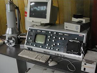

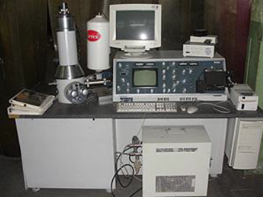

ID: 155989
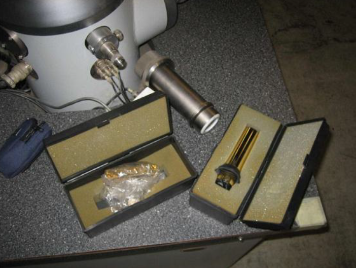
Scanning electron microscope
Upgraded EDS detector
Kevex data level 2 analysis
Spectrum analysis
EDS imaging
Included upgrades:
Upgraded Iridium II microanalysis system (EDS) in early 2000's with:
P/N 0627-92: Personal Computing System
P/N 0627-93: IXRF EDS Electronics
P/N 0627-77: IXRF High Voltage Supply
P/N 0627-95: IXRF PC Acquisition Interface
P/N 0627-96: Iridium Software Package
Imaging / x-ray mapping hardware and software
4k x 4k image acquisition elemental x-ray mapping feature analysis
Image processing
Upgrades provide the following capabilities:
X-ray mapping
Line scans
Position-tagged spectroscopy
Feature measurement
Image processing.
AMRAY 1000 is a scanning electron microscope (SEM) designed to provide high-resolution, three-dimensional imagery of a variety of sample types. The system uses a monochromatic electron beam - a beam of electrons with a single wavelength of energy - to image samples by means of surface interaction. A range of detector and scanning mechanisms enable the capture of images, in both two and three-dimensional form. 1000 features a high-resolution composite Cathode-Luminescence (CL) SEM detector with three modes of illumination, including high and low-angle reflection and dark-field imaging. This detector captures and interprets the signal produced when the scanning electron beam interacts with the samples. The data from the signal is then processed to form two-dimensional images and three-dimensional reconstructions. The data can also be further analyzed using analysis packages such as elemental mapping and surface composition analysis. The system's wide-field view chamber enables precision measurements to be taken on samples, with magnifications of up to 120,000x. This chamber also has the ability to induce secondary electrons to supplement the imaging resolution and the electron beam energy setting can be adjusted to achieve optimum performance. AMRAY 1000 offers repeatable results and is ideal for achieving reliable, high-resolution imaging. It is suitable for a large range of materials, including biological specimens and semiconductor samples, and is able to cope with a wide range of specimen surface shapes and sizes. The system utilizes a range of detectors, including secondary electron images (SEI), back-scatter electron images (BSEI) and transmission electron images (TEI), to allow for the capture of a range of images and data sets for analysis. Alongside imaging modes, 1000 also offers surface modification analysis through the addition of a range of imaging systems.
There are no reviews yet
