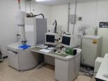
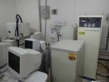
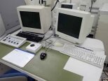
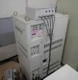
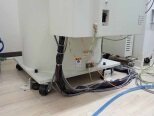
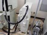
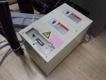
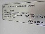
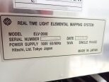
Used HITACHI HD-2000 #9234174 for sale
URL successfully copied!
Tap to zoom
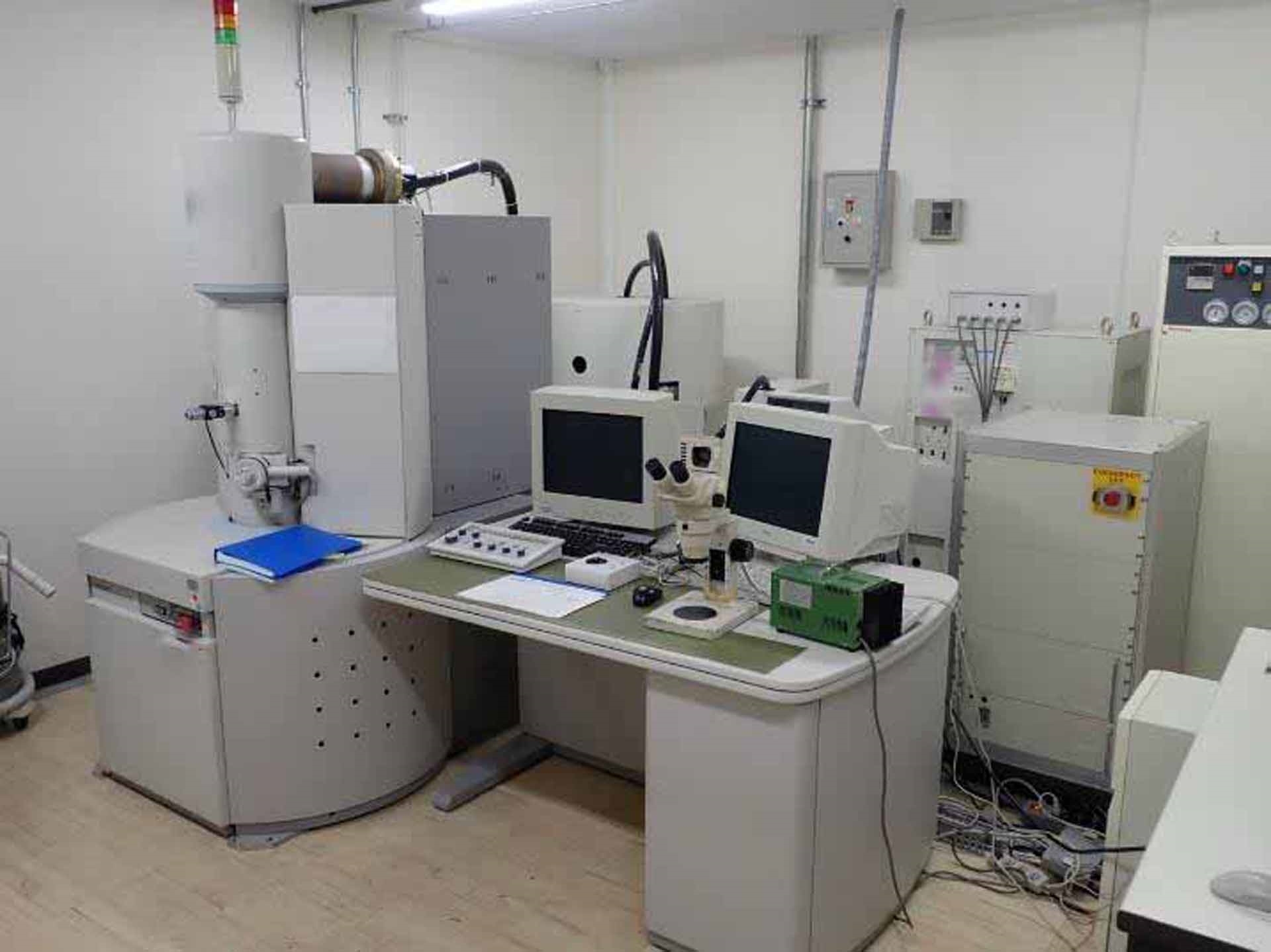

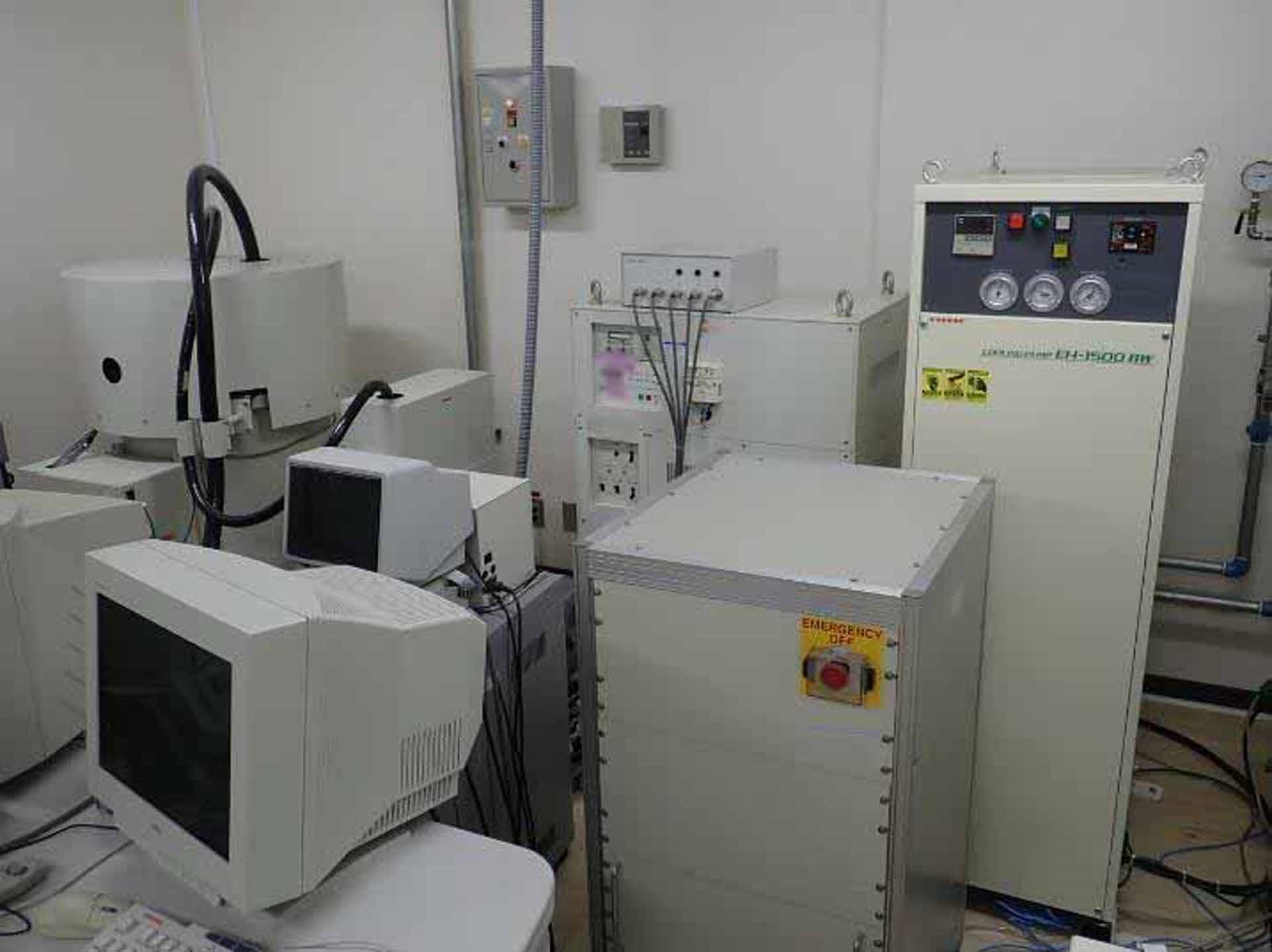

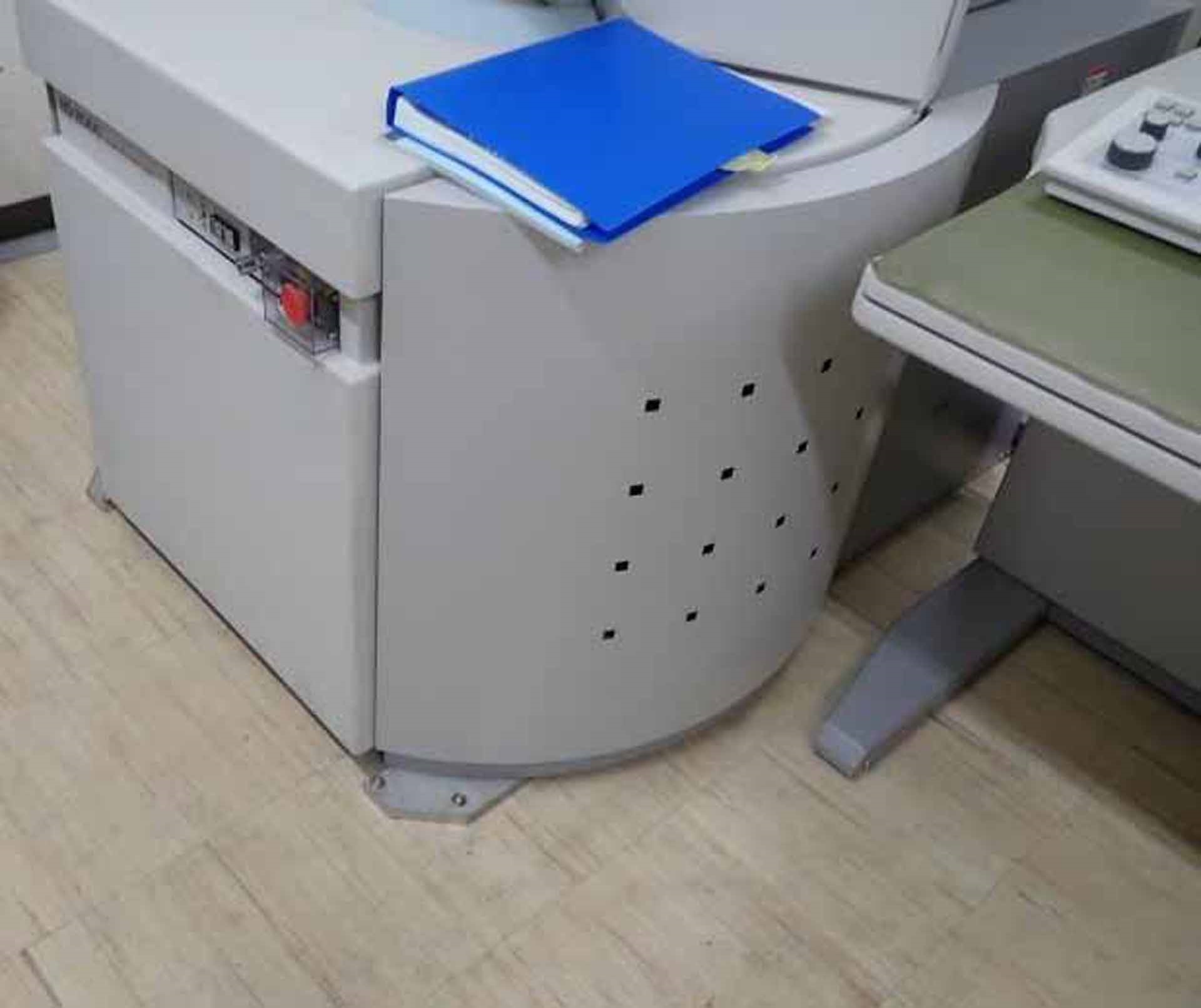

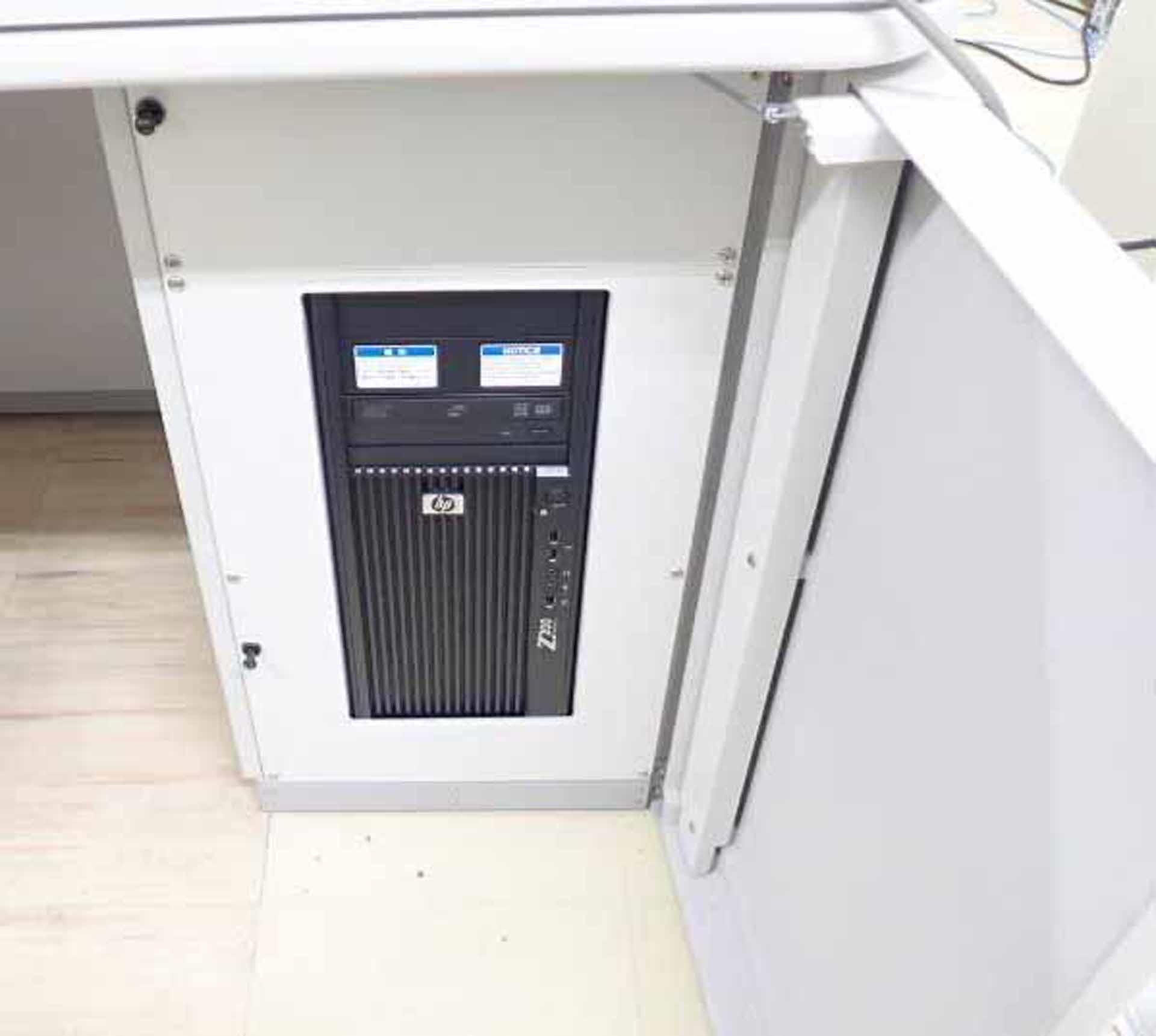

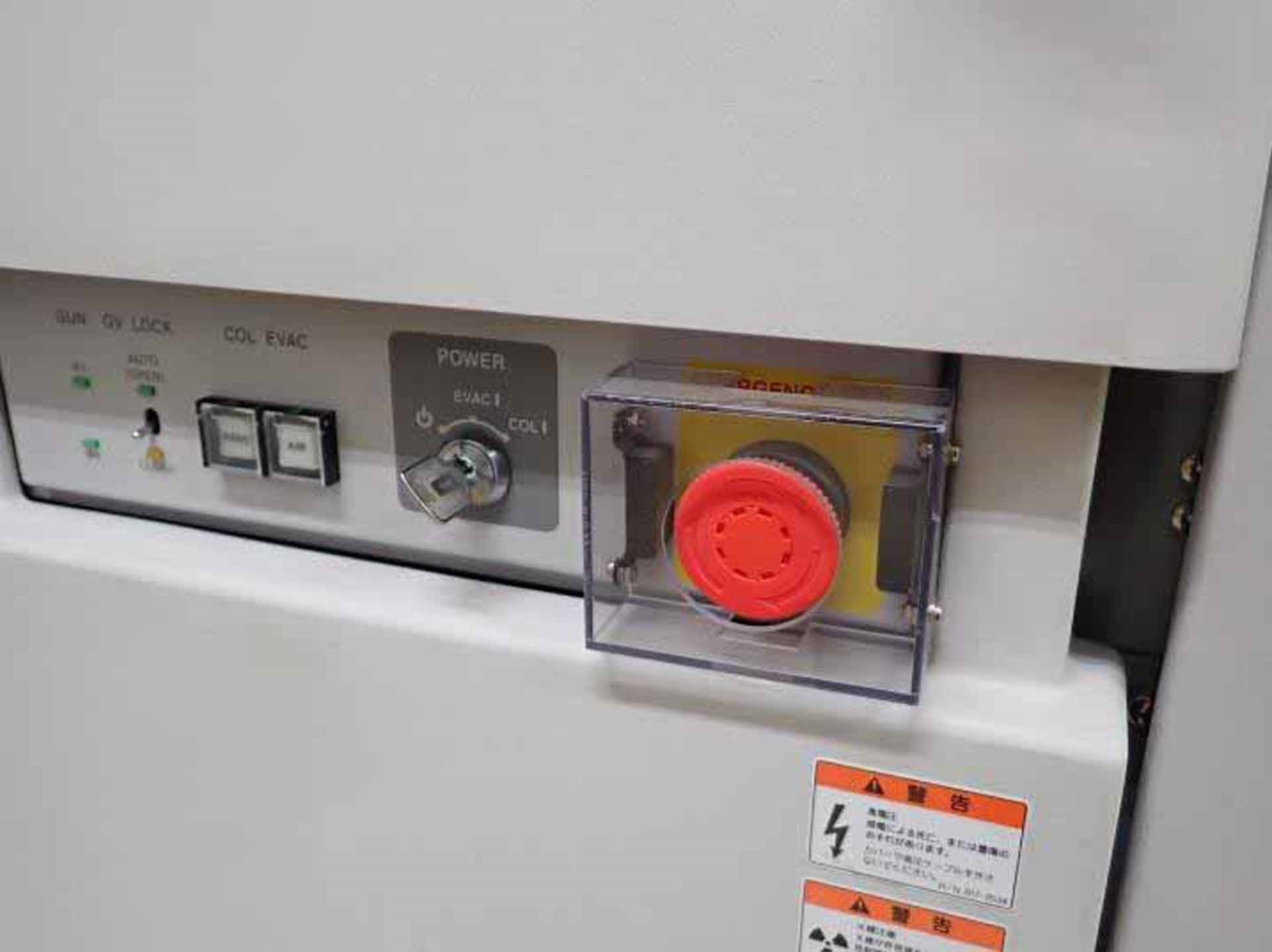

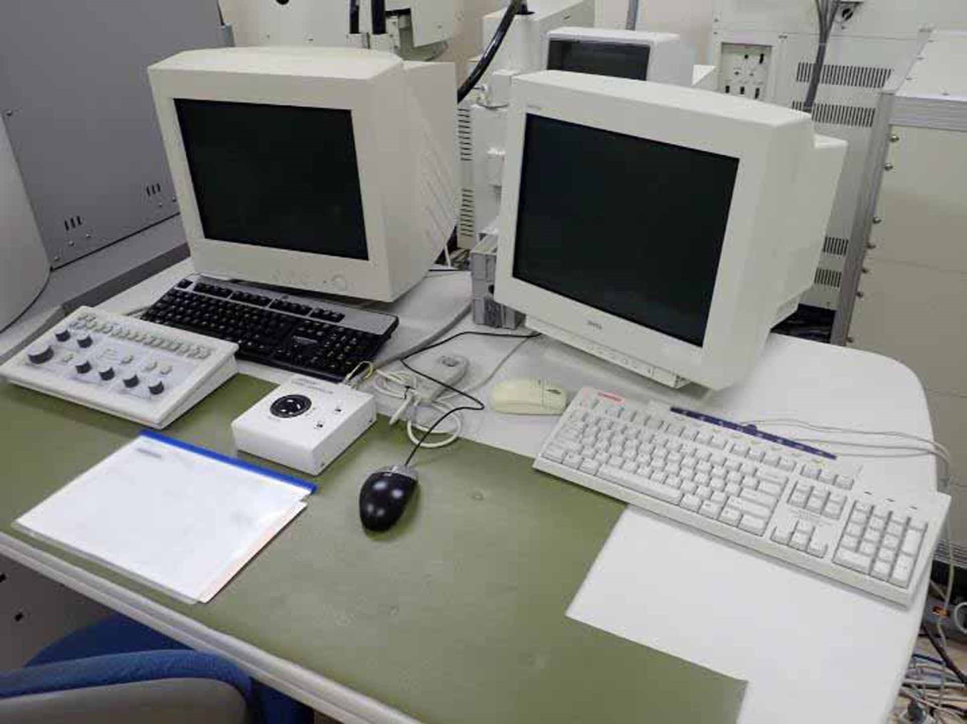






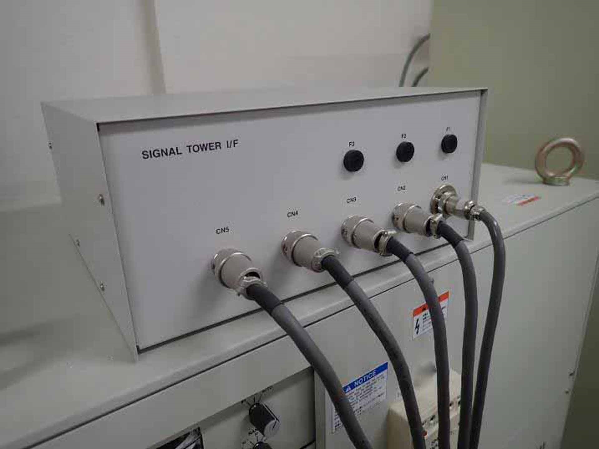



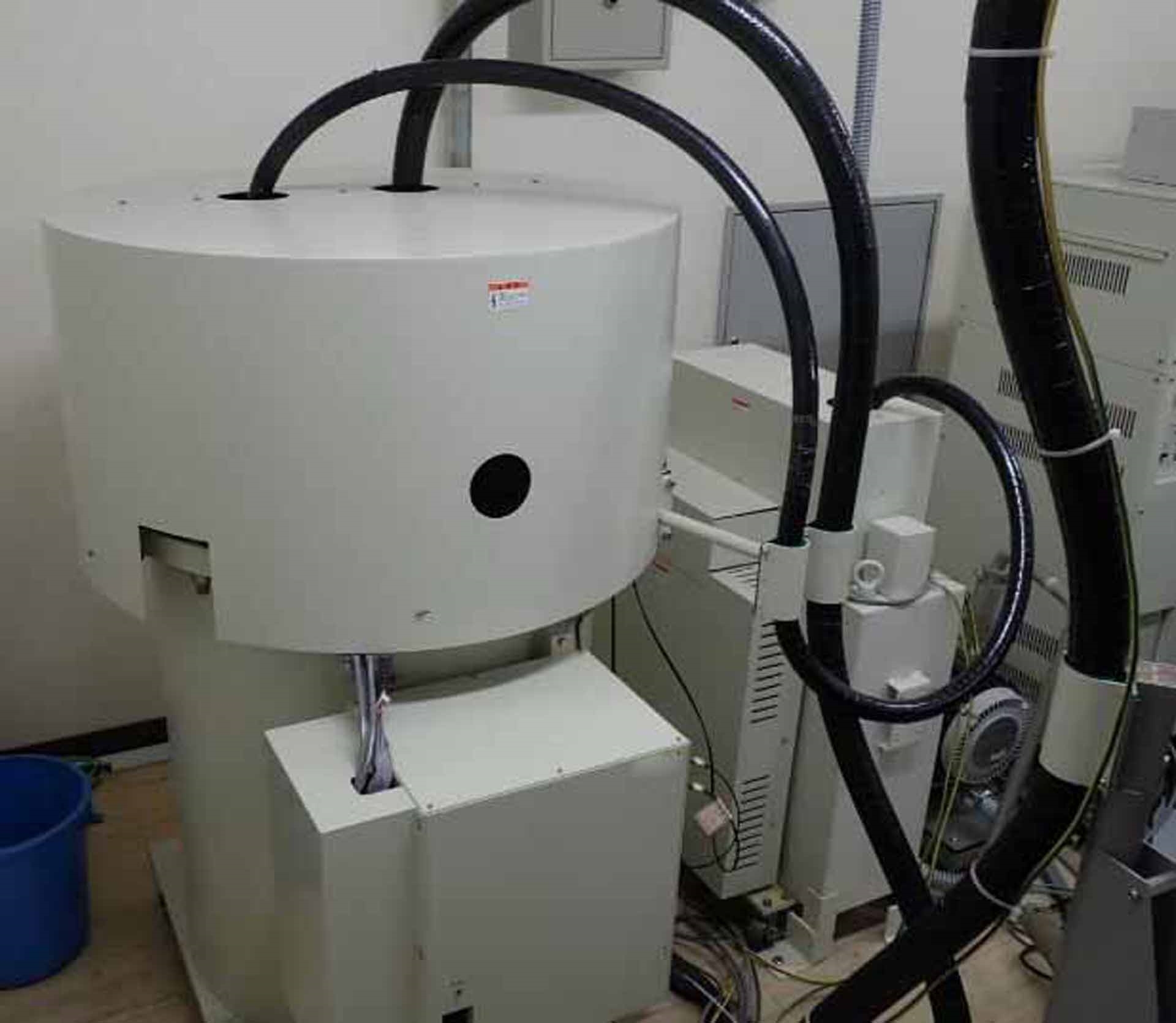

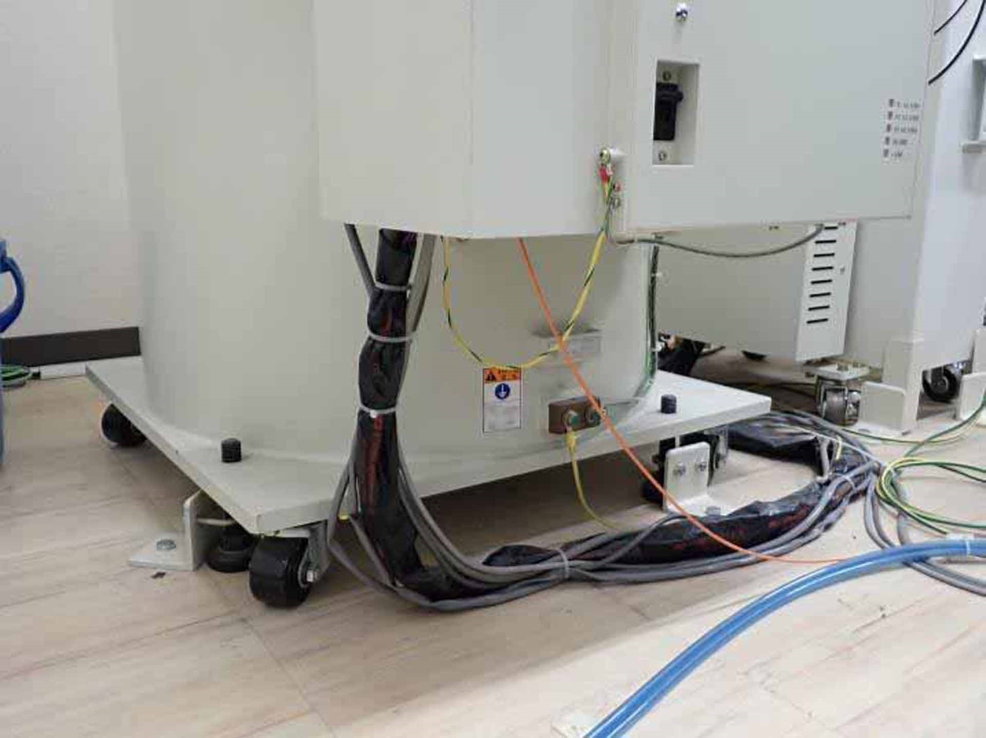

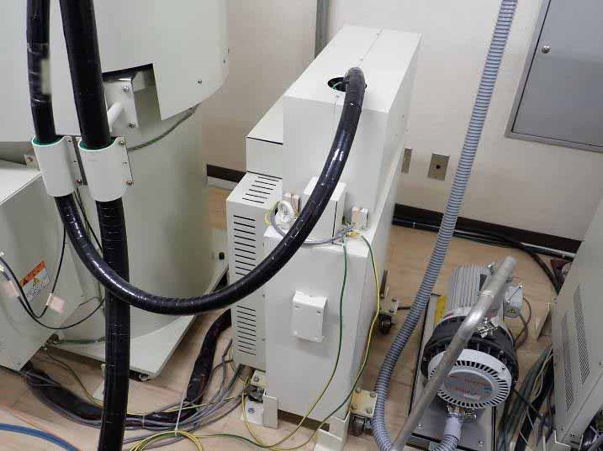

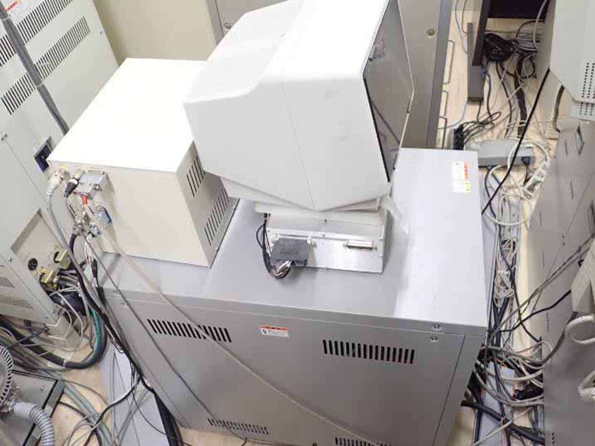






ID: 9234174
Vintage: 2001
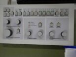
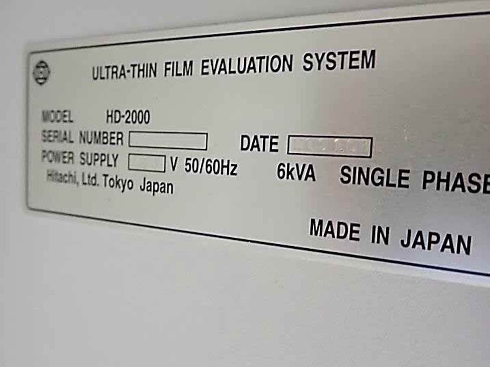
Ultra thin film evaluation system
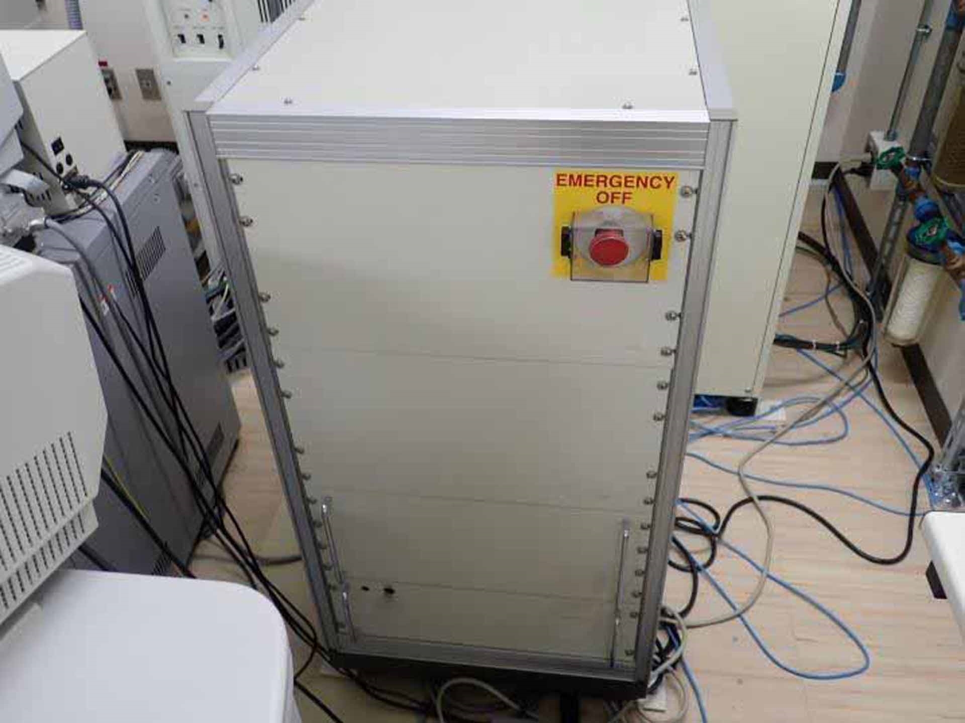
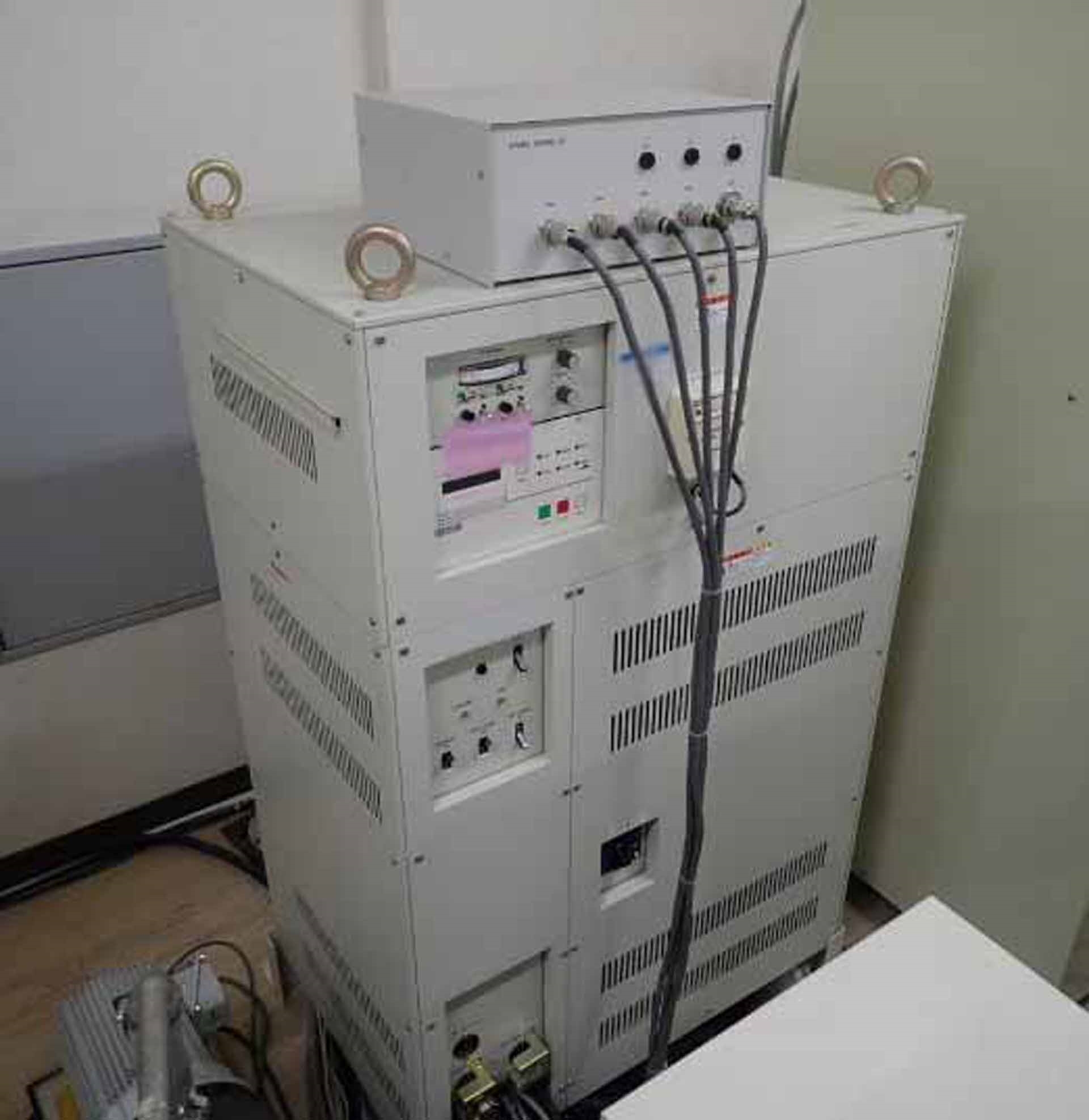
Includes:
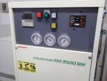
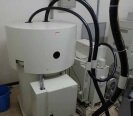
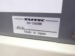
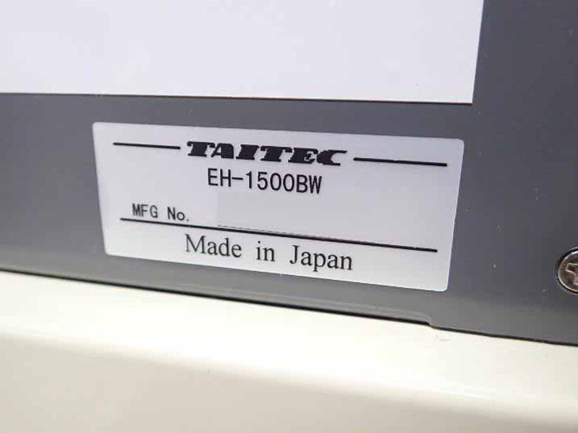
TAITEC EH-1500BW Cooling water circulation device
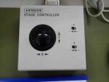
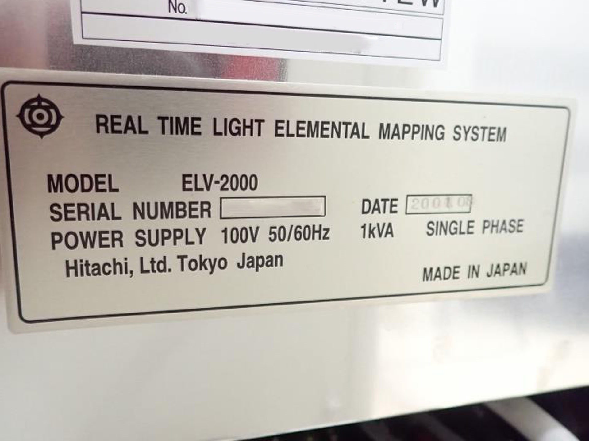
HITACHI ELV-2000 Scanning unit
PS Unit
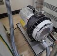
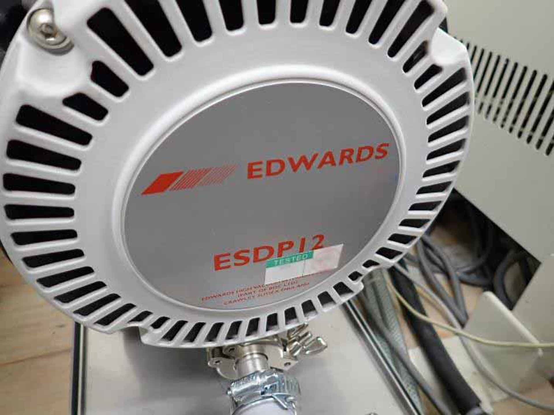
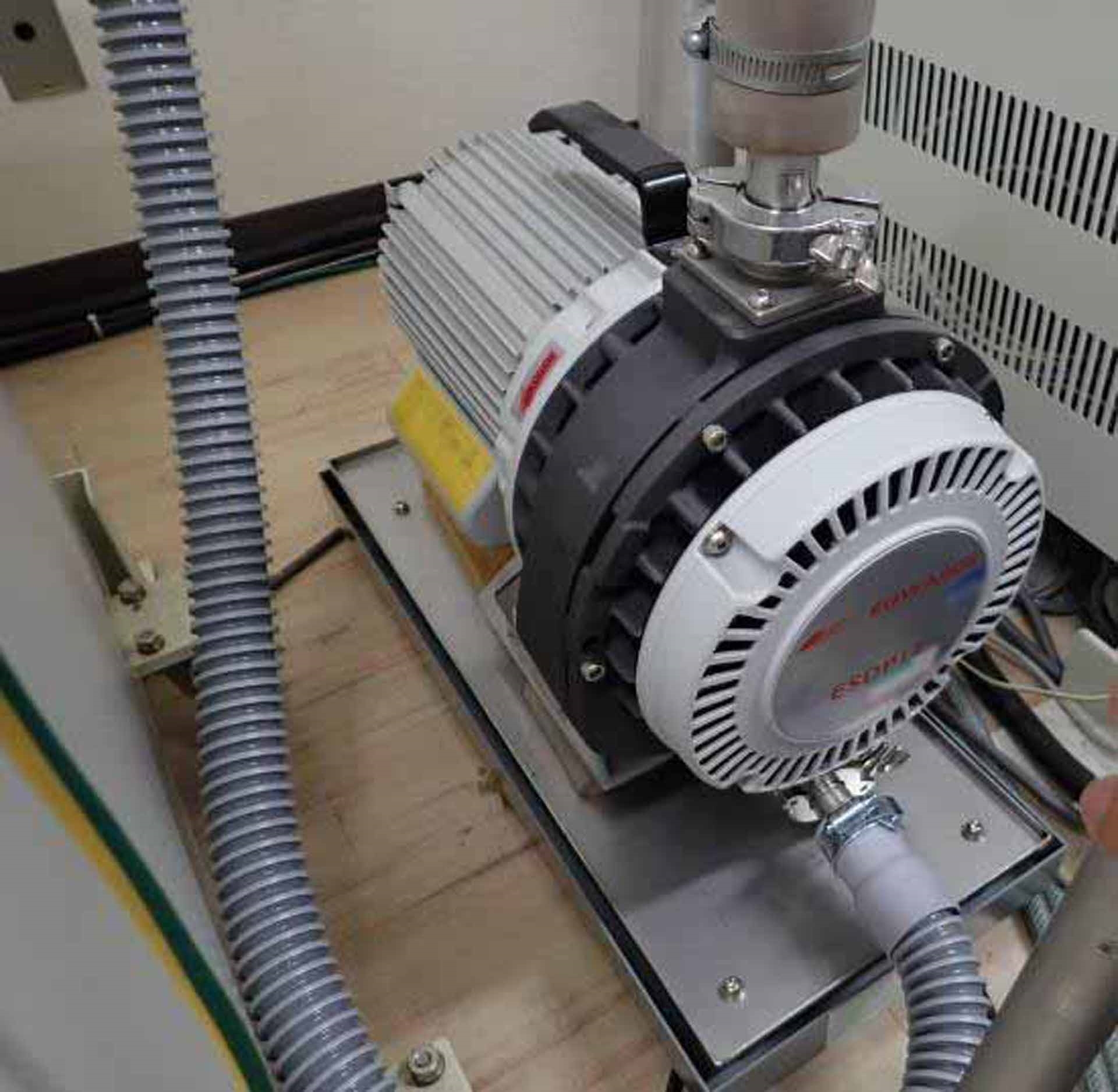
EDWARDS ESDP 12 Dry vacuum pump
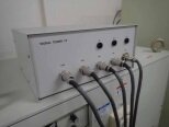
ORIGIN ELECTRIC FE Power supply
Mirror
Operating system: Windows 7
2001 vintage.
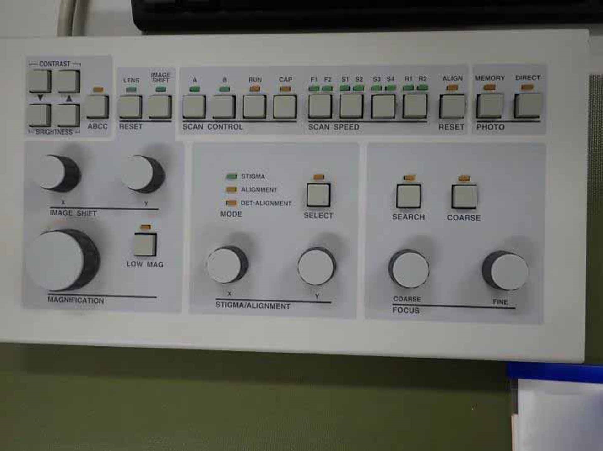
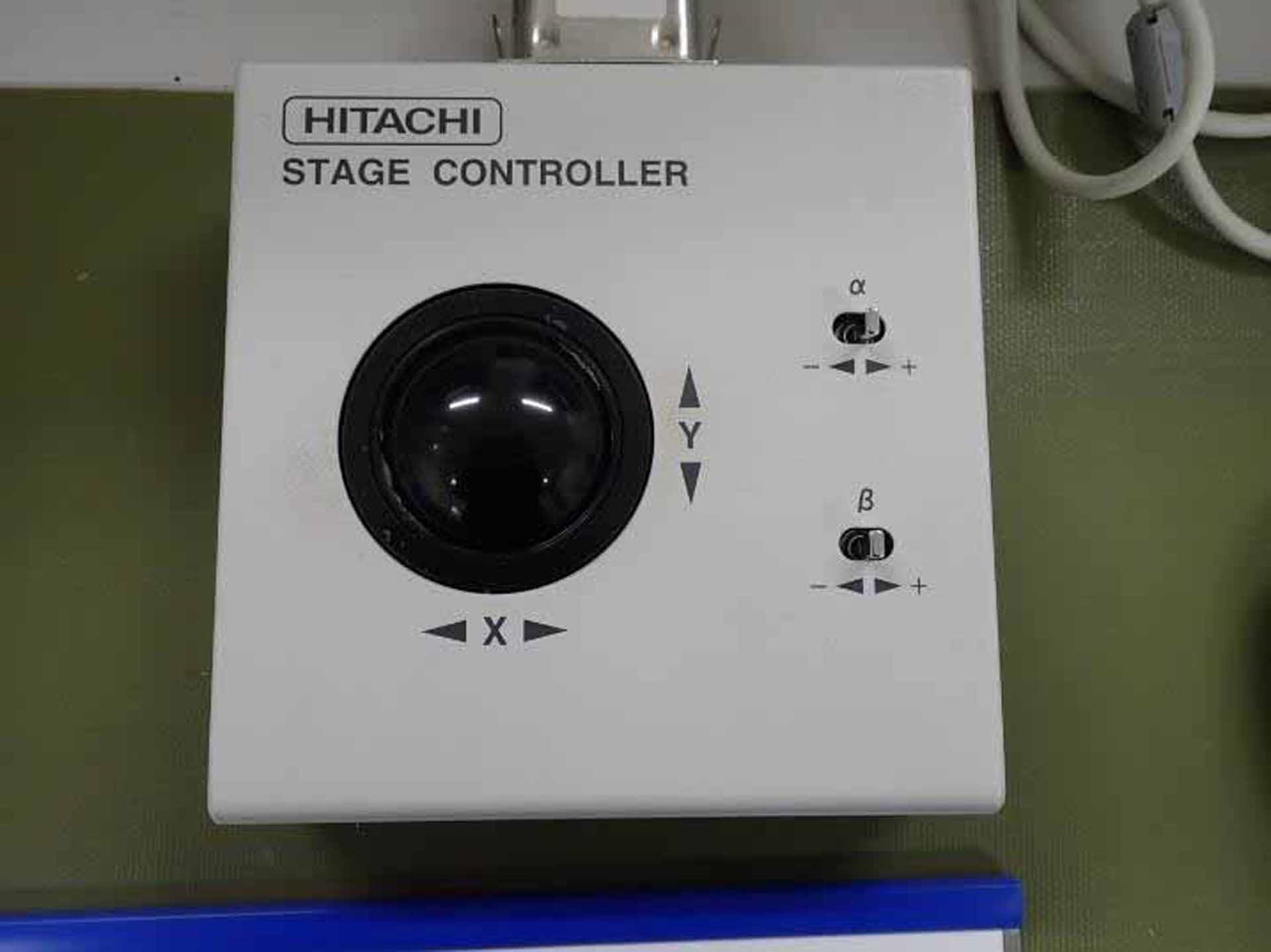
HITACHI HD-2000 is a Scanning Electron Microscope (SEM) designed for a wide range of materials and applications, including production and failure analysis, alloy and composition measurement, device characterization, and three-dimensional imaging. HITACHI HD 2000's integrated equipment includes a SEM with a high-resolution everhart-thornley type SE detector, an image-processing unit, a high-performance 2D cathodoluminescence imaging system, and a variety of sample holders. It also features a high-magnification EDX spectrometer (energy dispersive spectroscopy) which provides elemental analysis of sample surfaces at high resolution and sensitivity. HD-2000's low mass scanning stage offers fast scanning speed and excellent stability, while its low magnification imaging capability captures clear images in the nanometer range. It is also equipped with a high-precision piezoelectric Z-drive for accurate sample positioning and the highest resolution imaging. HD 2000's high resolution everhart-thornley detector produces clear images of sample surfaces and thin sections, even at large magnifications. Its ability to capture low-magnification images makes it an ideal tool for characterization of nano-devices. It can also be used in combination with an FEI SEM to provide three-dimensional imaging with sub-structure resolution. HITACHI HD-2000's high-performance cathodoluminescence imaging unit is used to collect a wide range of spectra and 3-dimensional distribution images of luminescent materials, including LED chips, photovoltaic elements, and high-precision optical components. HITACHI HD 2000's EDX spectrometer helps to quickly identify elemental composition by performing high-sensitivity and high-resolution analysis at kV energies from 0.5 keV to 20 keV. It can be used for alloy characterization, semiconductor films thickness analysis, and surface analysis with high-contrast images. In addition to its imaging capabilities, HD-2000's low mass scanning stage makes it an excellent tool for automated sample positioning and measurement. Its stage can handle multiple samples at a time, allowing users to load multiple samples without interruption. By quickly switching between samples, it can also support fast and efficient sample analysis. HD 2000 is an advanced and reliable scanning electron microscope, capable of quickly and accurately capturing images of the nanometer range. Its integrated machine includes a SEM, image processing unit, cathodoluminescence imaging tool, EDX spectrometer, and a low mass scanning stage. This scanning electron microscope is an ideal choice for materials and applications in production and failure analysis, alloy and composition measurement, device characterization, and three-dimensional imaging.
There are no reviews yet
