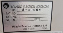
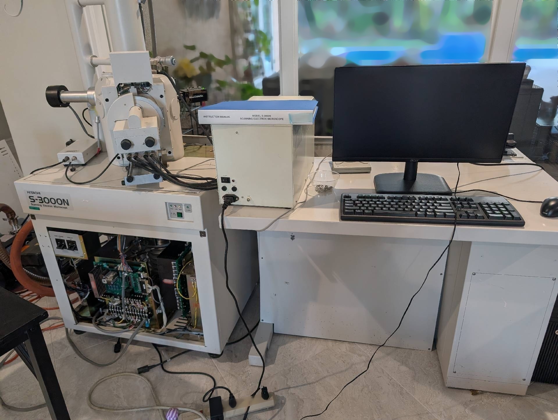
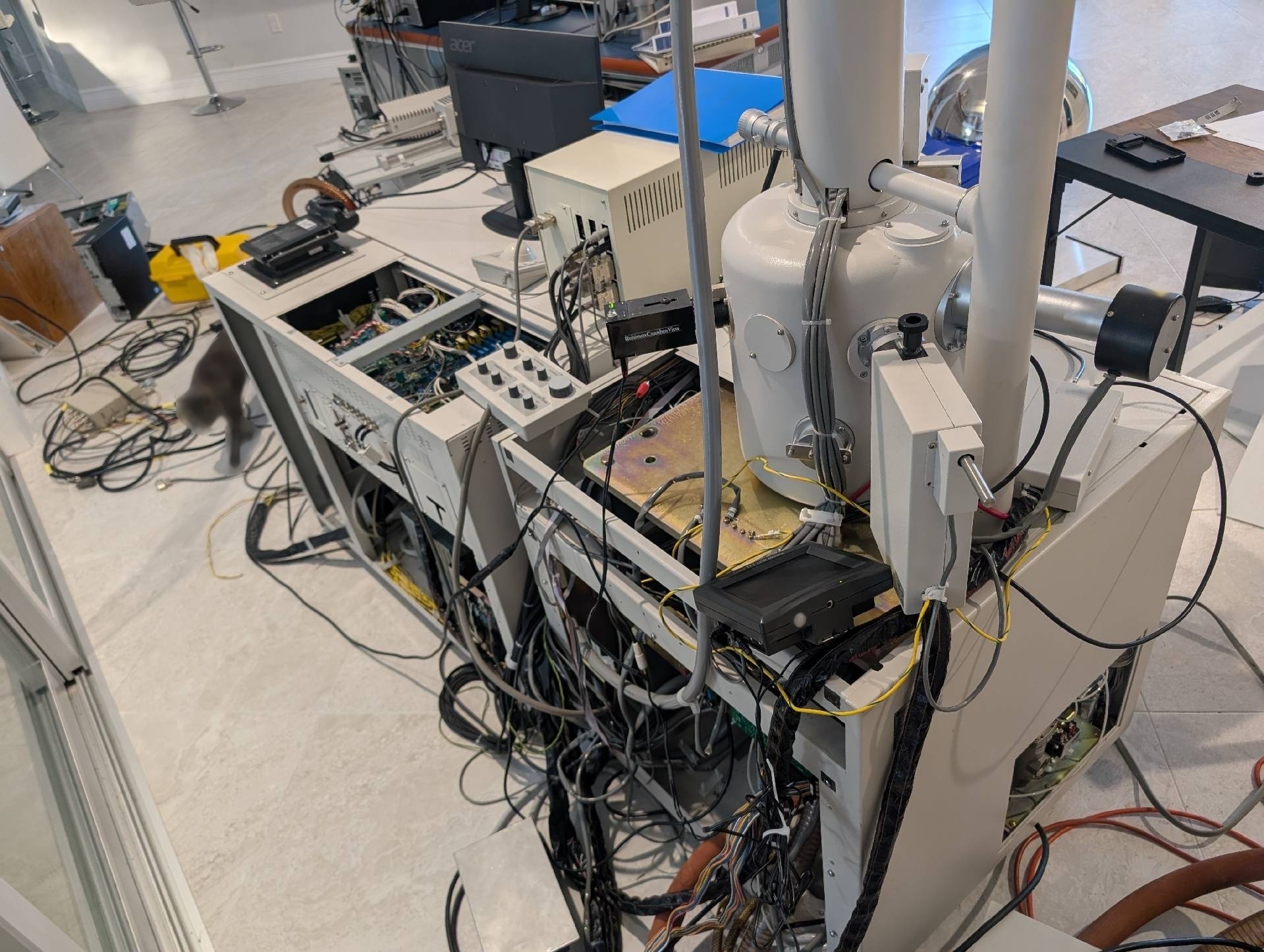
Used HITACHI S-3000N #293820636 for sale
URL successfully copied!



Tap to zoom


ID: 293820636
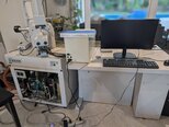
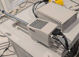
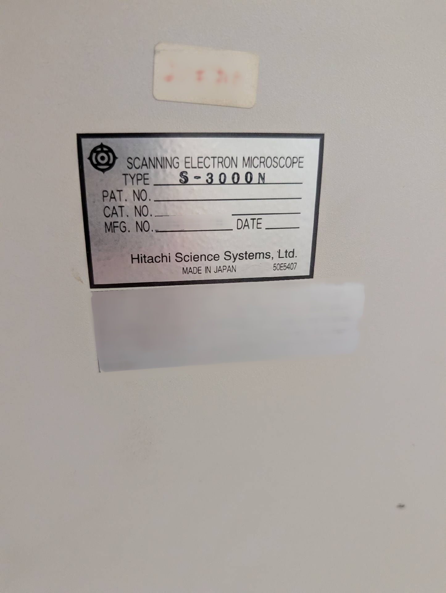
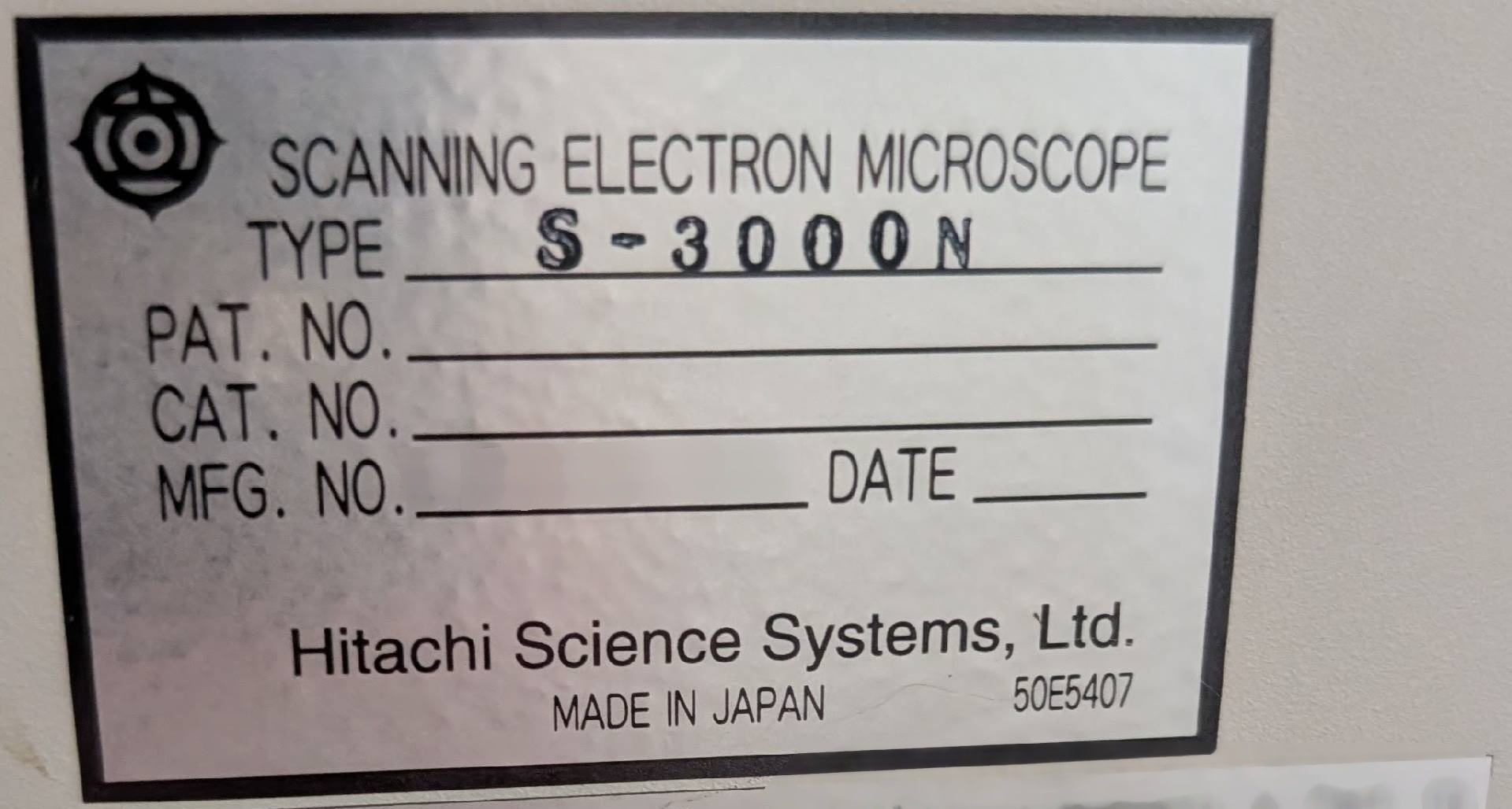
Scanning Electron Microscope (SEM)
Silicon Drift Detector (SDD)
Secondary electron (SE) image: 3.0–3.5 nm at 25–30 kV in high vacuum (HV) mode
Backscattered electron (BSE) image: 5.0 nm at 25 kV in variable pressure (VP) mode
Some sources note: ~15 nm SE at 3 kV (HV) or 5 nm overall in VP mode at 25 kV
Accelerating voltage: 0.3–30 kV
Magnification: 15× to 300,000× (normal mode, ~65 steps); low-mag mode down to 5× (75 steps)
Variable Pressure Range: 1 – 270 Pa (low vacuum/VP mode); high vacuum ultimate ~1.5 × 10⁻³ Pa
Maximum Specimen Size: 150–200 mm diameter; height typically up to ~20–40 mm
Working Distance (WD): Variable; X-ray/EDX optimized at 15 mm
Detectors:
Secondary electron detector (SE, high vacuum only)
Solid-state Backscattered Electron Detector (BSE, four-quadrant for compositional, topographic, or 3D modes; usable in HV and VP)
Absorbed current detector
Specimen Stage:
Common: X = 100 mm, Y = 50 mm, Z = 5–40 mm; tilt 0–60°; 360° rotation
Other options include super-eucentric, large eucentric, or 5-axis stages with different ranges (e.g., ±90° tilt possible on some)
Image Processing & Display:
Frame memory: 640×480 (display), 1280×960 (high-res), optional 2560×1920
Features: Auto brightness/contrast (ABC), auto focus/stigmator, image integration, gamma control, recursive filtering
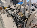
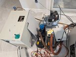
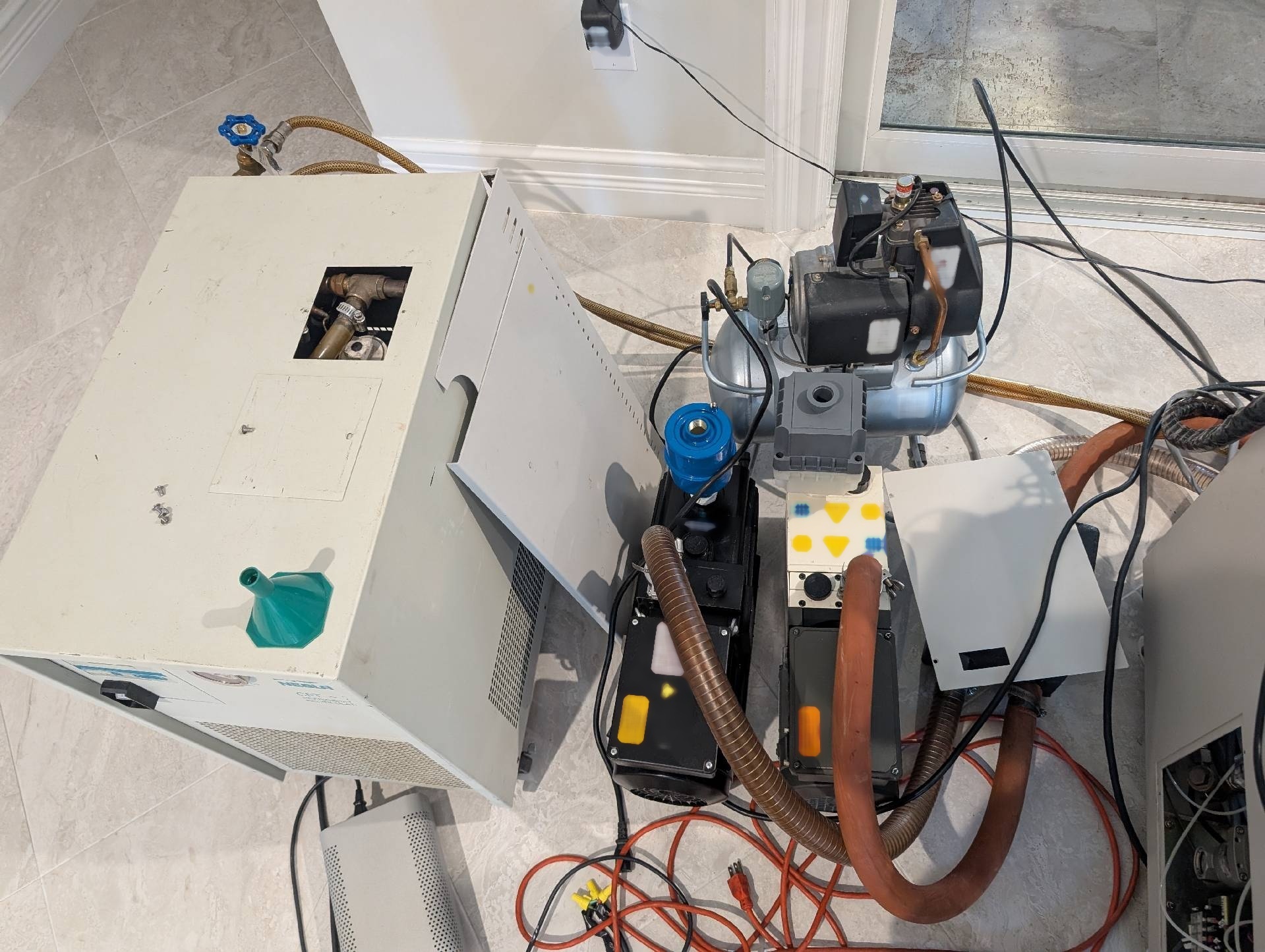
(2) Pumps
Chiller
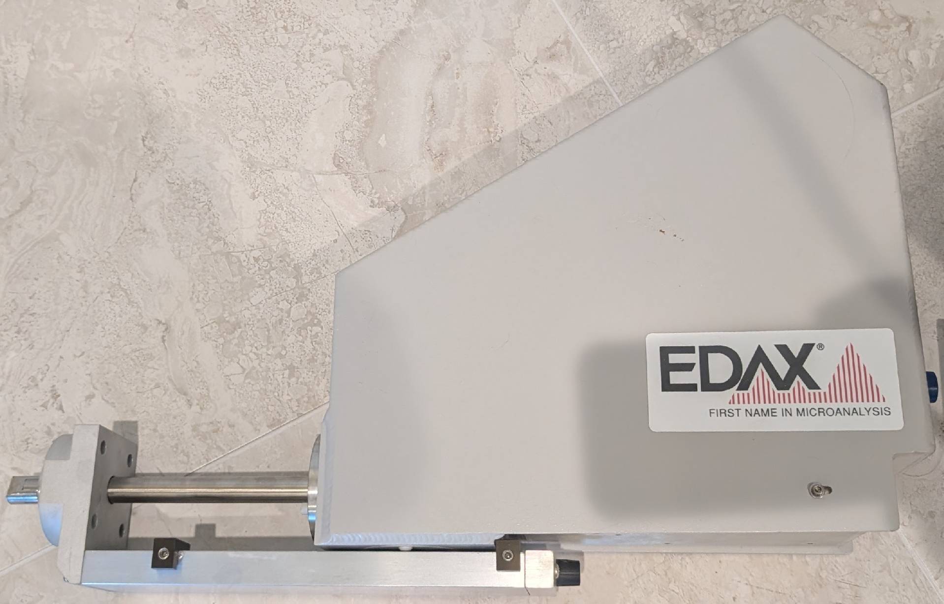
Spare manual stage
Motorized stage
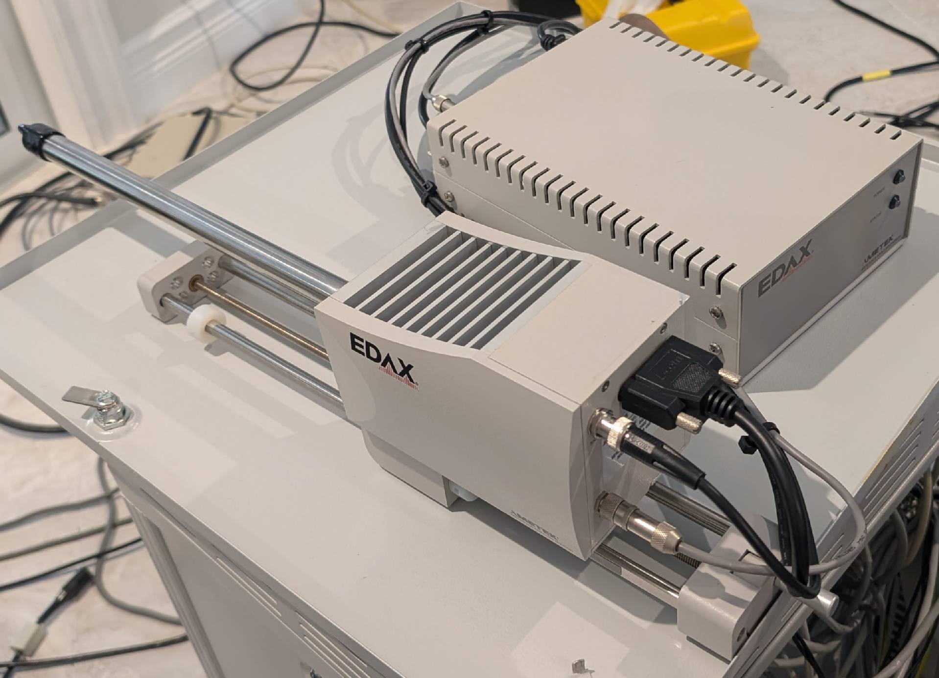
EDAX Si(Li) detector
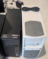
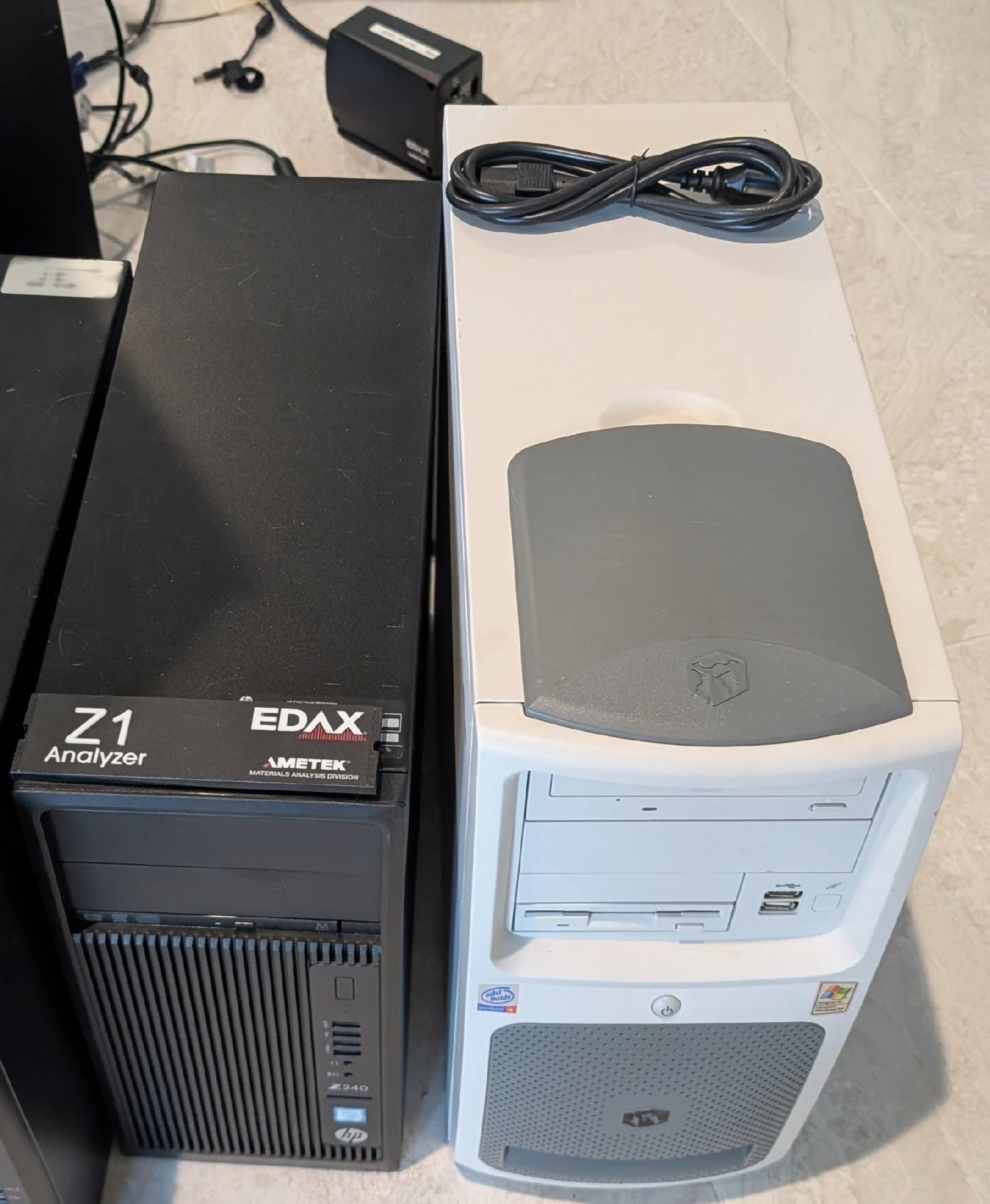
EDAX Falcon compute
EDAX Apollo EDS
Genesis computer.
HITACHI S-3000N is a scanning electron microscope (SEM) with remarkable capabilities for high-resolution imaging and analysis of samples on the nanoscale. Utilizing an advanced electron optics equipment, HITACHI S-3000 N produces images of superior spatial resolution and excellent contrast, with fast scan speeds. S 3000 N utilizes a unique dual SEM column which provides the ultimate in flexibility when it comes to increasing working distance, operating voltage, fields of view and magnification. The microscope's large working distance of 25mm enables analysis of thicker samples with greater stability, while the high-resolution electron optics system captures details with stunning clarity, making it suitable for imaging a range of objects from irregular shaped structures to ultra-fine features. HITACHI S 3000 N is equipped with an advanced spectral feature control unit that accurately identifies specimens, allowing for accurate analysis and accurate parameters for sample inspection. Additionally, the machine is capable of controlling the scanning electron current from 0.3nA to 1000nA, enabling analysis of different materials with different material characteristics. When it comes to analyzing specimens, S-3000 N offers two additional features: EDX and EBSD. These functions enable users to detect elements and measure crystallographic orientations on materials such as metals, ceramics and semiconductors. Equipped with a remarkable multichannel detector with high-speed counting capabilities, S-3000N can also perform best-in-class elemental mapping with fast imaging speeds. HITACHI S-3000N provides streamlined user ergonomics, with a comprehensive user interface allowing for easy settings and operation. For advanced users, the special ImageWare software package allows for remote operation as well as images processing with ease. For applications that require a scanning electron microscope with a high level of performance and flexibility, HITACHI S-3000 N is the ideal choice. With its wide range of capabilities and excellent imaging qualities, it is a powerful tool to successfully characterize many types of specimen and explore new nanoscale applications.
There are no reviews yet