Used HITACHI S-4500 #293804950 for sale
URL successfully copied!
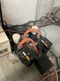
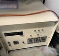
Tap to zoom
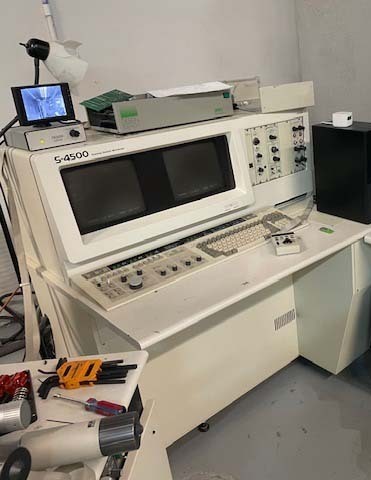

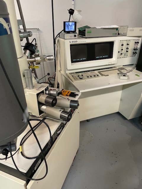
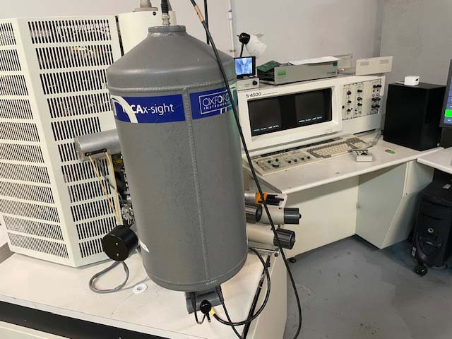
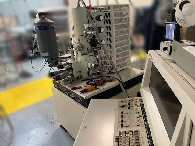
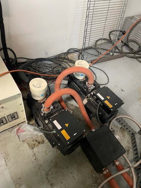
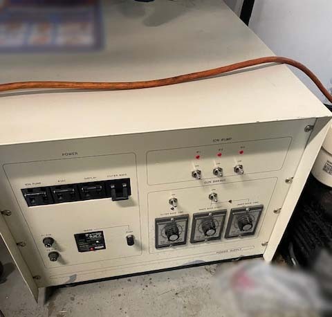
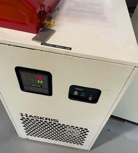
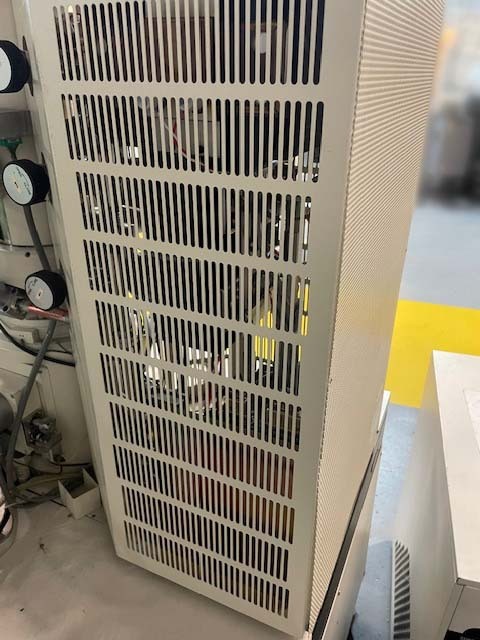
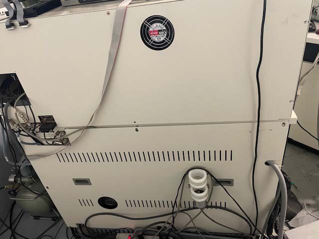
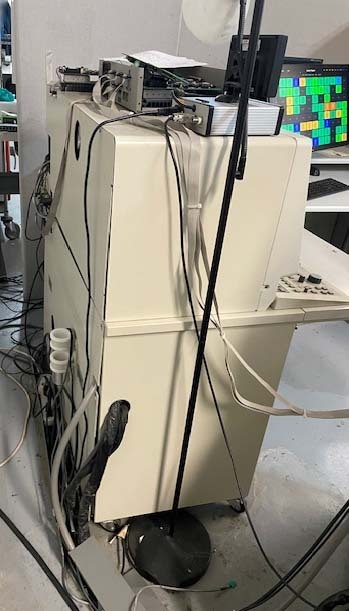
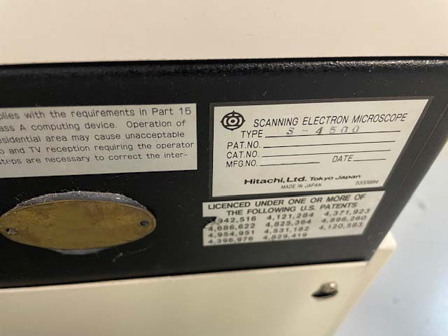
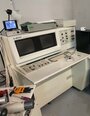
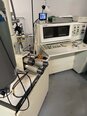
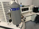
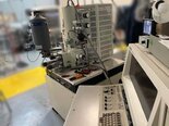
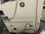
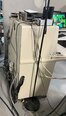
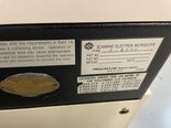
HITACHI S-4500 Scanning Electron Microscope (SEM) is an advanced instrument for high resolution imaging and analysis of many different kinds of material. It is designed for use in a wide variety of applications, from industrial quality control, to materials testing and research in the fields of microelectronics, life sciences, and bio-photonics. With its advanced design, HITACHI S 4500 provides superior performance in digital imaging, providing users with detailed information of their samples. S-4500 utilizes an optimized field emission source to provide excellent imaging resolution, making it well suited for a variety of fields from nanotechnology to material science. The detector design allows for clear imaging without the obscuring effects of diffraction. The microscope is able to amplify signals up to 200,000 times providing users with an extremely detailed representation of their sample. The equipment has a wide range of spot sizes, ranging from less than 0.5µm to 30µm, providing users the flexibility to accurately detect and analyze the structure of their sample. The state-of-the-art automation system of S 4500 enables the user to save and recall a variety of settings, such as magnification level, spot size, beam current, and exposure time. This greatly reduces user interaction time and provides near instant results. In addition, the microscope comes standard with an integrated digital image collection unit equipped with proprietary software to store images for further analysis. HITACHI S-4500 is also equipped with an adjustable stage, allowing for positioning of the sample with sub-micron precision. The sample can be manually manipulated or through the optional automated micromanipulation machine. High resolution imaging can be achieved through the use of specialized lenses, such as an in-column energy lens or an in-column field emission lens. HITACHI S 4500 is a high-precision tool tailored to meet the demands of professionals in many different fields. With its advanced imaging resolution, high automation, and optional micromanipulation tool, the SEM provides a reliable and efficient way to study intricate and nanostructured material.
There are no reviews yet