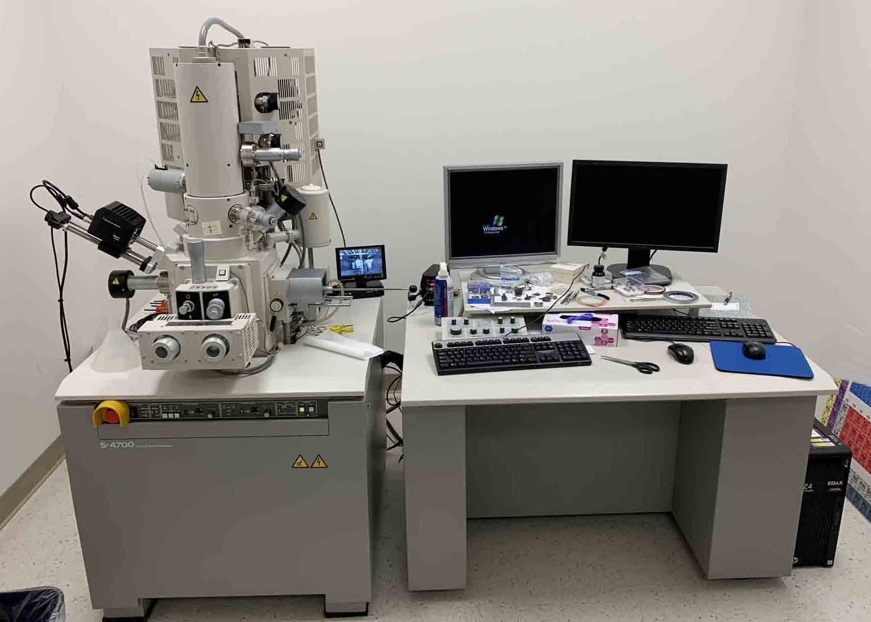
Used HITACHI S-4700 #9241883 for sale
It looks like this item has already been sold. Check similar products below or contact us and our experienced team will find it for you.
Tap to zoom


Sold
ID: 9241883
Scanning Electron Microscope (SEM)
Resolution:
1.5 nm with 15 kV beam, 12 mm working distance
2.1 nm with 1 kV beam, 1.5 mm working distance
Magnification:
High mag mode: 100x - 500,000x
Low mag mode: 20x - 2,000x
Electron optics:
Electron gun: Cold cathode field emission type
Extracting voltage (Vext): 0 to 6.5 kV
Accelerating voltage (Vacc): 0.5 to 30 kV
Lens: 3-Stage electromagnetic lens
Objective lens aperture:
Movable aperture
Self-cleaning thin aperture
Astigmatism correction coil (stigmator): Electromagnetic type
Scanning coil: 2-Stage electromagnetic deflection type
Specimen stage:
X Range: 0 to 25 mm
Y Range: 0 to 25 mm
Z Range: 1.5 to 26.5 mm
Tilt range: -5 to 45 degrees
Rotation: 360 degrees
Spec. size: Maximum100 mm diameter
Display options:
Scanning speeds:
Live viewing: 0.5 to 40 sec per frame
Photo: 17 - 333 seconds per frame
Electrical image shift: 15 um at 12 mm
Evacuation system:
Ultimate vacuum levels
Specimen chamber: 7E^-4 Pa
Electron gun chamber: 2E^-7 Pa at ion pump 1
Vacuum pumps:
Electron optics: (3) Ion pumps
Specimen chamber: Oil diffusion pump or turbo molecular pump
(2) Oil rotary pumps
Acoustic noise: Less than 65 dB
Dielectric voltage-withstand: 1500 VAC/1 min
Microscope control OS: Windows XP
Does not include EDAX.
HITACHI S-4700 is a scanning electron microscope (SEM) that is used for visualizing nanoscale objects and materials. It provides high resolution images with unsurpassed image sharpness, comparable to conventional laboratory light microscopes without the need for applied contrast agents. The SEM operates in two modes: Scanning Mode and Point Mode. In Scanning Mode, a homogenized beam of electrons is emitted from the electron gun and focused on the sample by a series of electromagnetic lenses. As the beam scans the sample, the electrons are collected backscattered and then detected in an electron detector. This allows for the formation of a digital image of the sample with ultrahigh resolution. The Point Mode SEM produces a single tightly focused electron beam that can be used to locate and analyze individual areas of interest on the sample and generate extremely high-resolution images of the features present. This enables the user to perform precise and accurate measurements of dimensions, shapes and other characteristics. HITACHI S 4700 also has various detector configurations and advanced imaging methods to enable the user to observe a wide variety of materials and their properties. The SEM's built-in analytical capabilities include electron energy-loss spectroscopy (EELS) and energy-dispersive X-ray spectroscopy (EDS). With EELS, the user can use the scattered electrons from an accelerating voltage to measure the loss in energy of the electrons and identify the atoms that make up the sample. With EDS, X-rays are emitted from the sample to provide elemental information about the sample's composition. S-4700 works seamlessly with all of HITACHI imaging systems, allowing the user to quickly and easily perform imaging, analysis, and data processing. The controller and software provide automated operations, allowing the user to quickly identify, measure and analyze features on the sample and export the results. S 4700 is the ideal tool for research laboratories working in the nanotechnology, materials science, and life sciences fields; as well as producing highly accurate images and data on the nanoscale.
There are no reviews yet