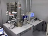
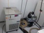
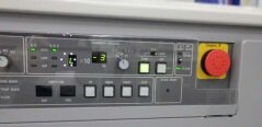
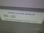
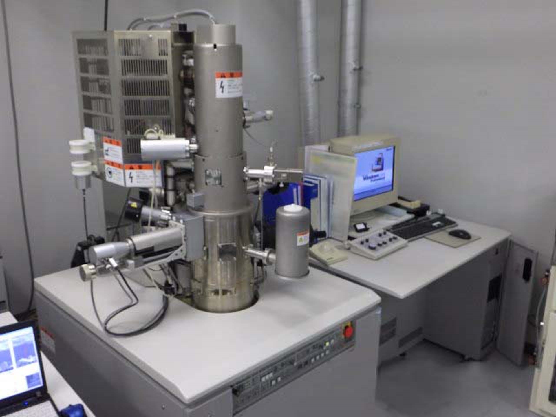
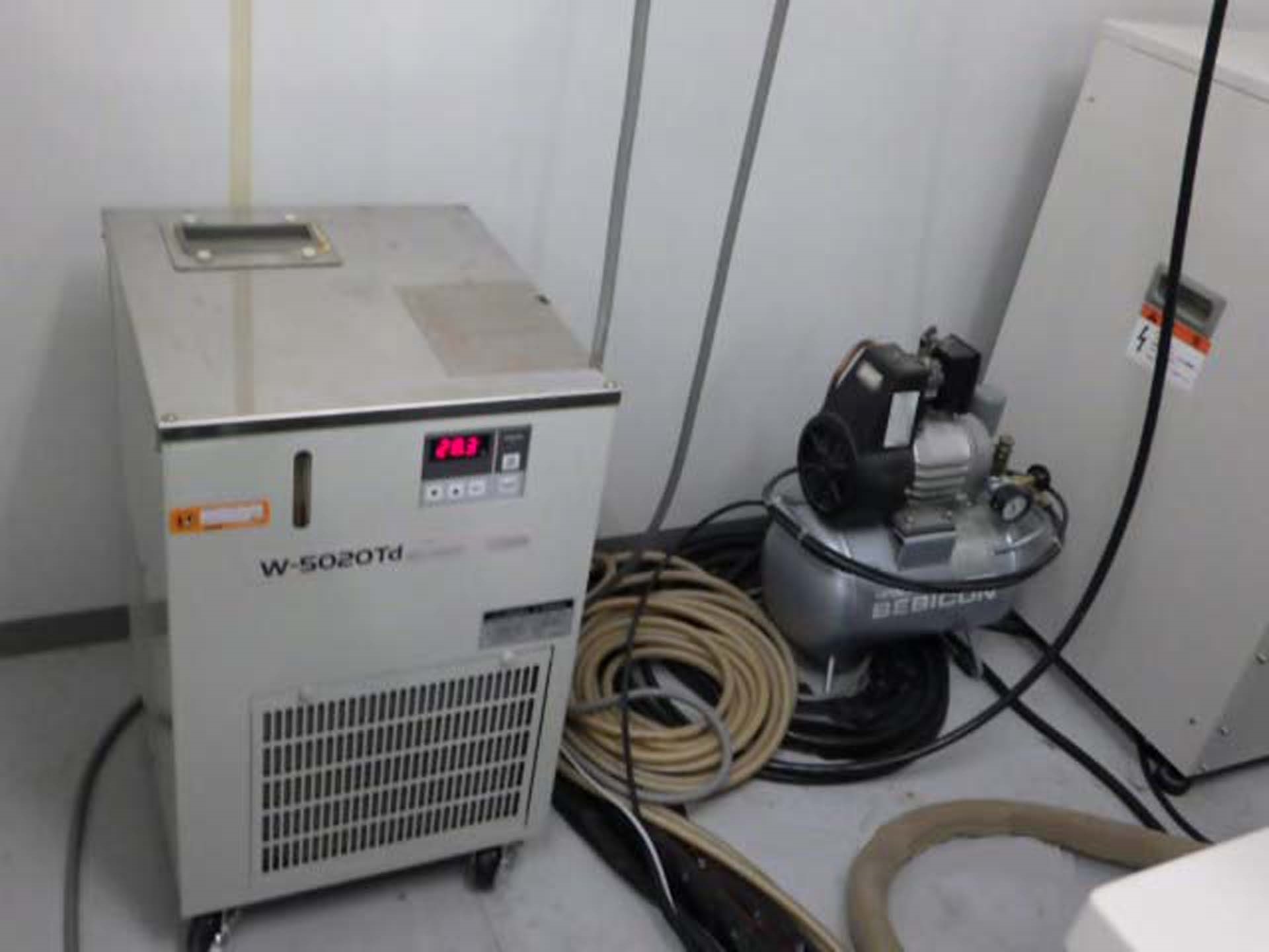
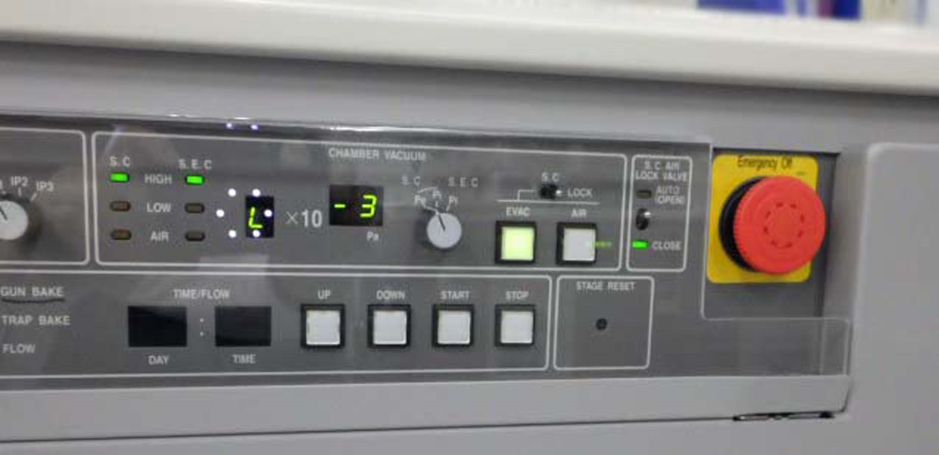
Used HITACHI S-5200 #9236135 for sale
URL successfully copied!
Tap to zoom




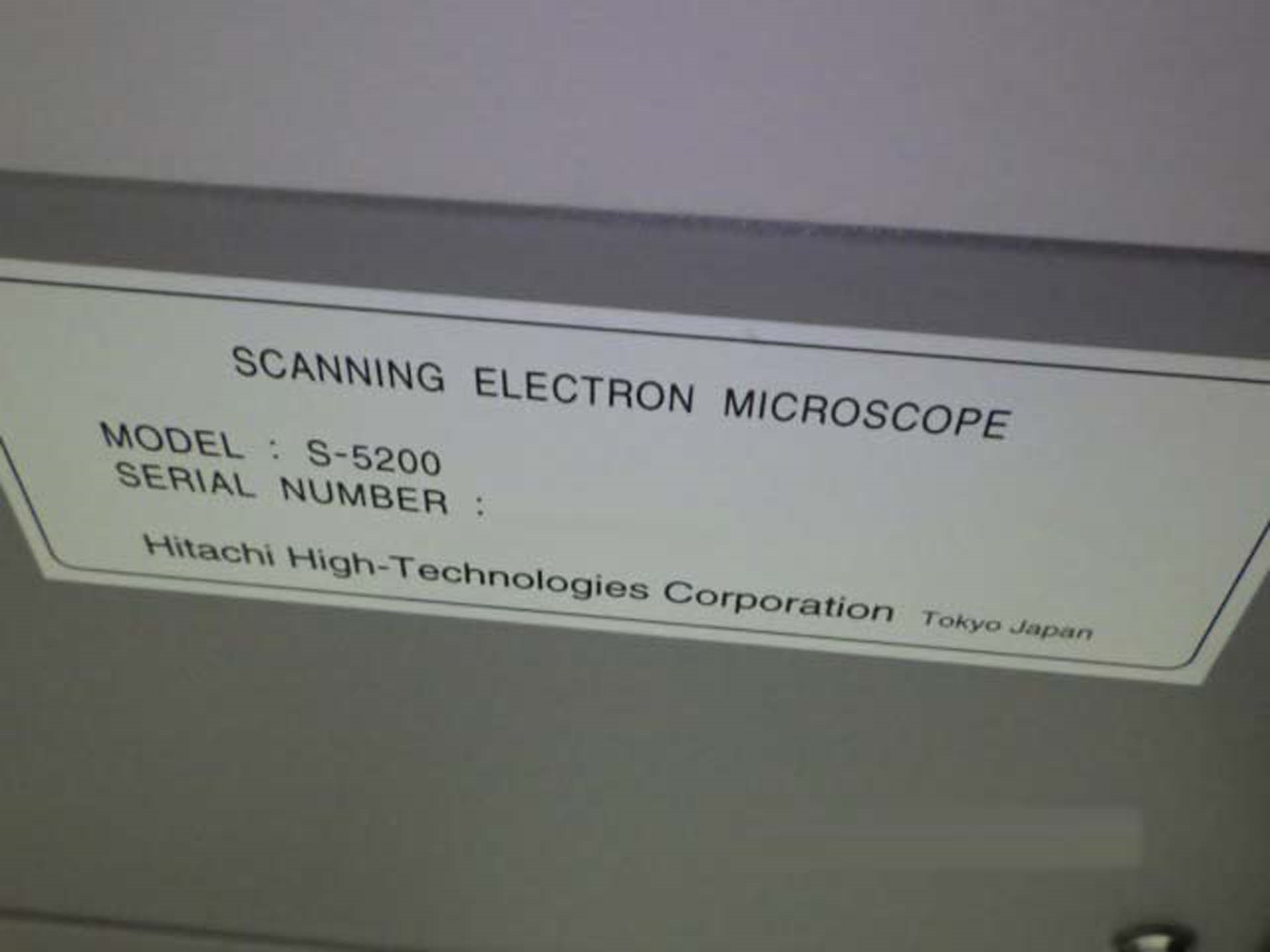

ID: 9236135
Vintage: 2003
Field Emission Scanning Electron Microscope (FE-SEM)
Resolution:
0.5nm (Accelerating voltage 30kV), Sample height: 0.5mm
1.8nm (Accelerating voltage 1kV), Sample height: 1.5mm
Magnification:
High magnification mode: ~800 x 2,000,000
Low magnification mode: ~60 x 10,000
Electric gun type: Cold cathode field emission electric gun
Extraction voltage (Vext): 0 ~ 6.5kV
Acceleration voltage: 0.5 ~ 30kV
Lens: 3-Stage electromagnetic lens reduction system
Objective lens aperture: Variable aperture
Astigmatic correction: Electromagnetic method
Scanning coil: 2-Stage electromagnetic deflection system
Sample fine movement apparatus:
X: +/- 3.5mm
Y: +/- 2mm
Z: +/- 0.3mm
T: +/- 40°
2003 vintage.
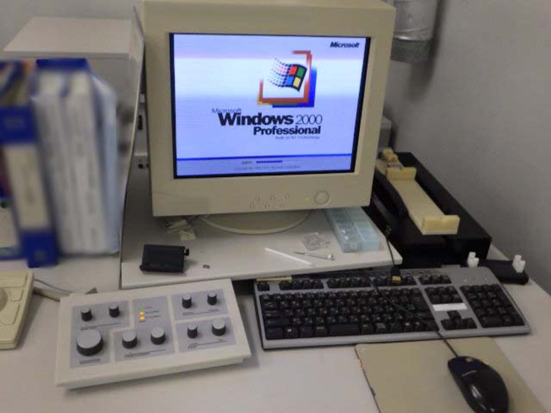
HITACHI S-5200 Scanning Electron Microscope (SEM) is a powerful imaging instrument for imaging the surface of specimens at the atomic or nanometer scale. This microscope combines high resolution imaging with fast acquisition rates making it ideal for a wide range of research applications. Its primary imaging technique utilizes a scanning electron beam and collects secondary electrons emitted from the sample to form an image. Secondary electrons can be collected with accelerated voltages of up to 30 kV which enables the observation of fine surface features of up to 10 nm. HITACHI S 5200 is capable of imaging a range of samples including biological and inorganic samples in both dry or wet conditions. The equipment also includes light elements detection and ptychographic imaging capability as well as in-built ion beam milling capabilities for bulk samples. It has an intuitive control system with a graphical user interface. Magnifications of up to xx,xxx can be achieved and resolution of better than 0.1nm. Accessories such as a range of stages, goniometers and environmental cells are also available to aid in the analysis of samples. The unit has a built-in energy-dispersive X-ray spectroscopy (EDS) detector, which enables the analysis of element distribution in the sample. Images collected by the EDS detector are combined with an electron image to produce a combined elemental distribution map. This capability makes S-5200 well suited for imaging applications in fields such as material science and nanotechnology. S 5200 also includes built-in digital video output capabilities for viewing live or captured images on external monitors. This feature is useful for sharing images with large groups of people. Software is provided to allow users to image and analyse samples with ease. It includes features such as real-time processing and measurements. In conclusion, HITACHI S-5200 Scanning Electron Microscope provides unparalleled imaging capabilities at the nanometer scale. It has a range of features that make it useful for a wide range of research applications and is highly automated and user friendly. The combination of imaging and analytical functions makes this machine one of the most powerful instruments available on the market today.
There are no reviews yet
