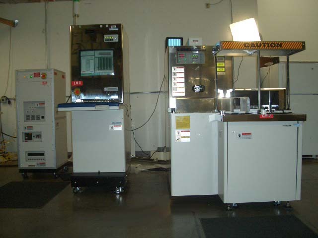
Used HITACHI S-8840 #139927 for sale
URL successfully copied!
Tap to zoom


ID: 139927
Wafer Size: 3"-8"
CD SEM, 8"
Upgraded to 3" to 8" wafer capability
CD measuring size: 130-160nm, consistently
Version 11.7 S/W or newer
SECS/GEM Communication Interface
Additional hard disk drive (>1GB)
VRT board w/ 8 mb of memory
DSP compatible conductive wafer holder
Hitachi Hi Tech Electron Gun
Accelerating voltage, 500V to 1300V, 10V steps
Probe current, 1-16pA at 800V, 1-10pA at 1000V, 1-13pA at 1300V
3 Stage Electromagnetic Lens System
Objective Lens: 4 opening click stop, heated aperture is selectable/adjustable outside the vacuum system
2-Stage Deflection Scan Coil
Astigmatism correction via an 8-pole electromagnetic coil
Magnification = 1000x to >150000x
Field control method ; Continuously on for sample decharging, at all voltages
Wafer imaging ability; Entire surface of 8"" wafer
Depth of focus: >= 1.0mm at 80000x magnification
Resolution: < 8nm at 700V - 1000V (or < 6nm with optional retarding voltage), < 6nm at 1000V - 1300V
Retarding voltage: Optional at <= 800V for improved resolution
Hitachi Probe Tip
Optical Microscope System: Image is Monochrome, using CCD camera, Magnification is 110x, Wafer imaging X & Y coverage from 5-195mm , notch down
Dual XY Hitachi Microscale
Workstation, HP B180L
Error Tracking Software
Multipoint Measurement Function
Edge Roughness Function
Contact Hole Measurement Function
Automated Image Archiving Function
Ergonomic Cassette Flipper Option (2 flippers - one per load port)
Operations Manual and Documentation.
HITACHI S-8840 scanning electron microscope (SEM) is one of the most advanced scanning electron microscopes available on the market and is often used for materials characterization and research. It is a modern, high-end SEM which can provide detailed images and data about the surface of a wide variety of materials, including semiconductors and ceramics. HITACHI S8840 SEM has a variety of features that sets it apart from other SEMs on the market. The microscope is equipped with a high resolution imaging system that provides a maximum resolution of 0.50nm and features Digital Signal Processing (DSP) technology. The imaging operation is automated, enabling the user to acquire high quality images without having to manually adjust the settings. Furthermore, the SEM features energy dispersive x-ray (EDX) spectroscopy which is used to identify the chemical composition of the samples being analyzed and detect element mapping. S 8840 is equipped with a powerful electron source which allows it to have superior performance in a wide range of applications. It also supports advanced analytical techniques such as 3D reconstruction and in-depth imaging. The microscope also has advanced operator control and user-friendly functions, as well as a comprehensive range of automation options. In addition to this, the microscope is equipped with an automated sample loader so the user does not have to manually prepare each sample for analysis. The high quality of imagery provided by S8840 enables the user to observe the most detailed features of a sample, and it is suitable for a wide range of applications. For example, the microscope can be used to study materials and nanostructures at a microscopically precise level, allowing the user to investigate the atomic structure of a sample as well as its surfaces and composition. Furthermore, the machine also has several imaging modes available, including scanning transmission electron microscopy (STEM), environmental sample chamber, fly-scan imaging, tilt scanning, and varying magnification scanning. Overall, S-8840 scanning electron microscope is an ideal choice for those looking for a high-end SEM that provides superior features and superior imaging capabilities. With its advanced features and powerful electron source, the microscope can provide precise and detailed images quickly and easily. Furthermore, its automation options and access to a variety of analytical modes make it an excellent choice for a wide range of research and studies.
There are no reviews yet