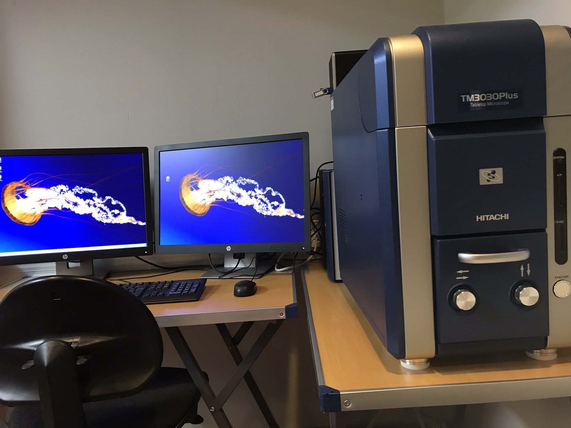
Used HITACHI TM-3030 Plus #9229603 for sale
It looks like this item has already been sold. Check similar products below or contact us and our experienced team will find it for you.
Tap to zoom


Sold
HITACHI TM-3030 Plus Scanning Electron Microscope (SEM) is a powerful imaging tool designed to offer high resolution imaging capabilities and precise measurements at the nano-scale. It is capable of creating detailed 3D images and has been specifically designed for materials characterization, failure analysis, and research applications. TM-3030 Plus is equipped with four electron sources: a Schottky Field Emission (SFE) FEG source, a Tungsten (W) FEG source, a Thermal Field Emission (TFE) source, and an In-column Lanthanum Hexaboride (LaB6) source. The System also has a Dual Detector system, which provides simultaneous operation of both an InLens Detector and a BackScattered Electron (BSE) Detector to allow for a variety of high resolution imaging modes. HITACHI TM-3030 Plus also has a user friendly GUI which simplifies operation of the system. The SEM also features a highly robust design which is engineered to withstand high vacuum conditions for a long time, making it ideal for prolonged characterization and imaging of nanostructures and sub-micron particles. The SEM is also highly reliable and produces low field emission currents, enabling it to provide images of high molecular and atomic resolution. Additionally, TM-3030 Plus utilizes angular filtering to reduce the influence of contaminant particles on the specimen being analyzed, resulting in a more detailed image. It is also capable of operating in large range of operating pressure settings and speeds, making it suitable for various cryo imaging applications. Furthermore, HITACHI TM-3030 Plus is equipped with a gentle beam approach to minimize sample damage during imaging, allowing for imaging of fragile specimens. The SEM also operates at full range of accelerating voltages, offering high-resolution imaging capabilities. Overall, TM-3030 Plus is a powerful All-in-One scanning electron microscope for materials characterization, failure analysis, and research applications. The SEM provides high resolution imaging capabilities, robust design, low field emission currents, and is equipped with multiple electron source and detectors for different imaging modes. Additionally, it is also capable of cryo imaging applications and features gentle beam approach to minimize sample damage during imaging.
There are no reviews yet