Used JEOL JBX-5500FS #293775451 for sale
URL successfully copied!
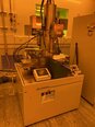

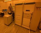
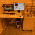
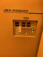
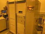
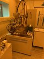
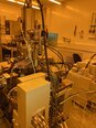
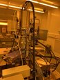
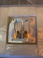
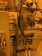
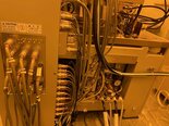
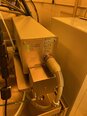

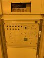
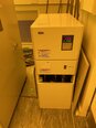
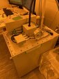
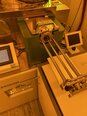




Tap to zoom
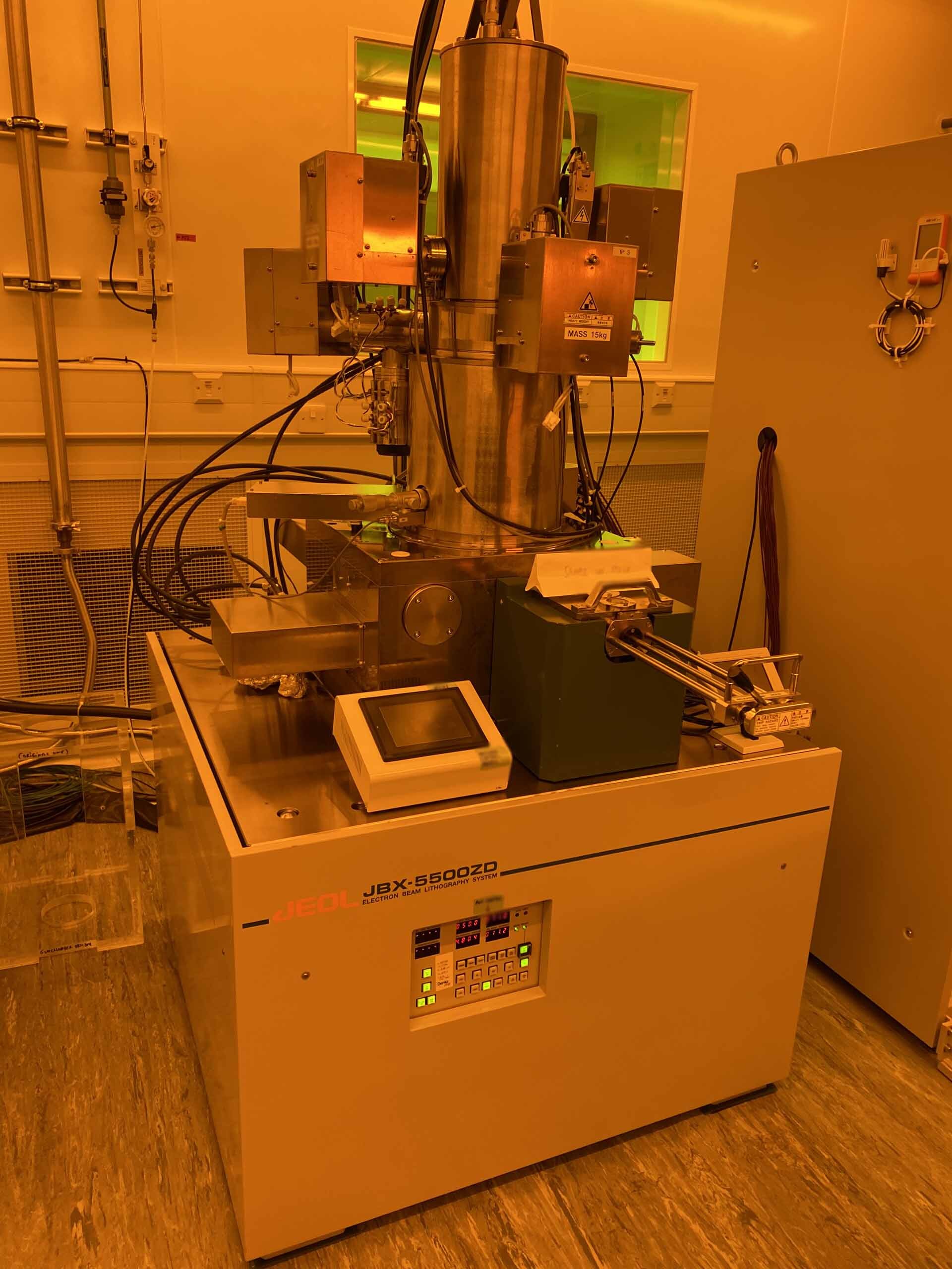

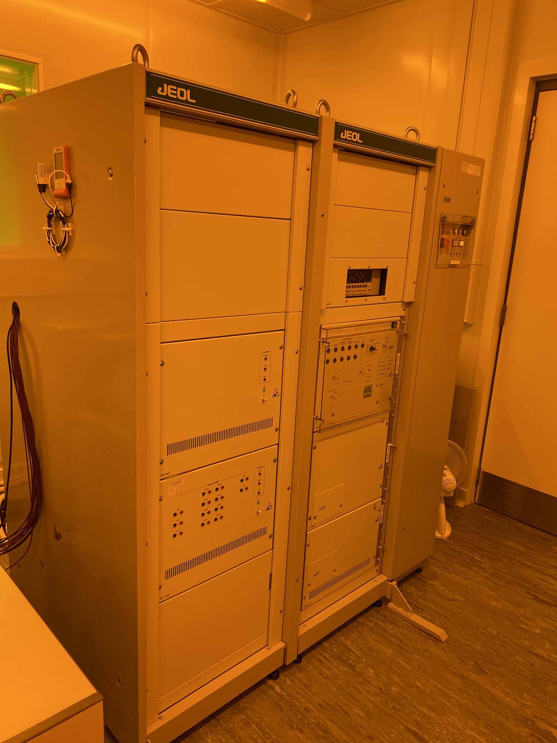
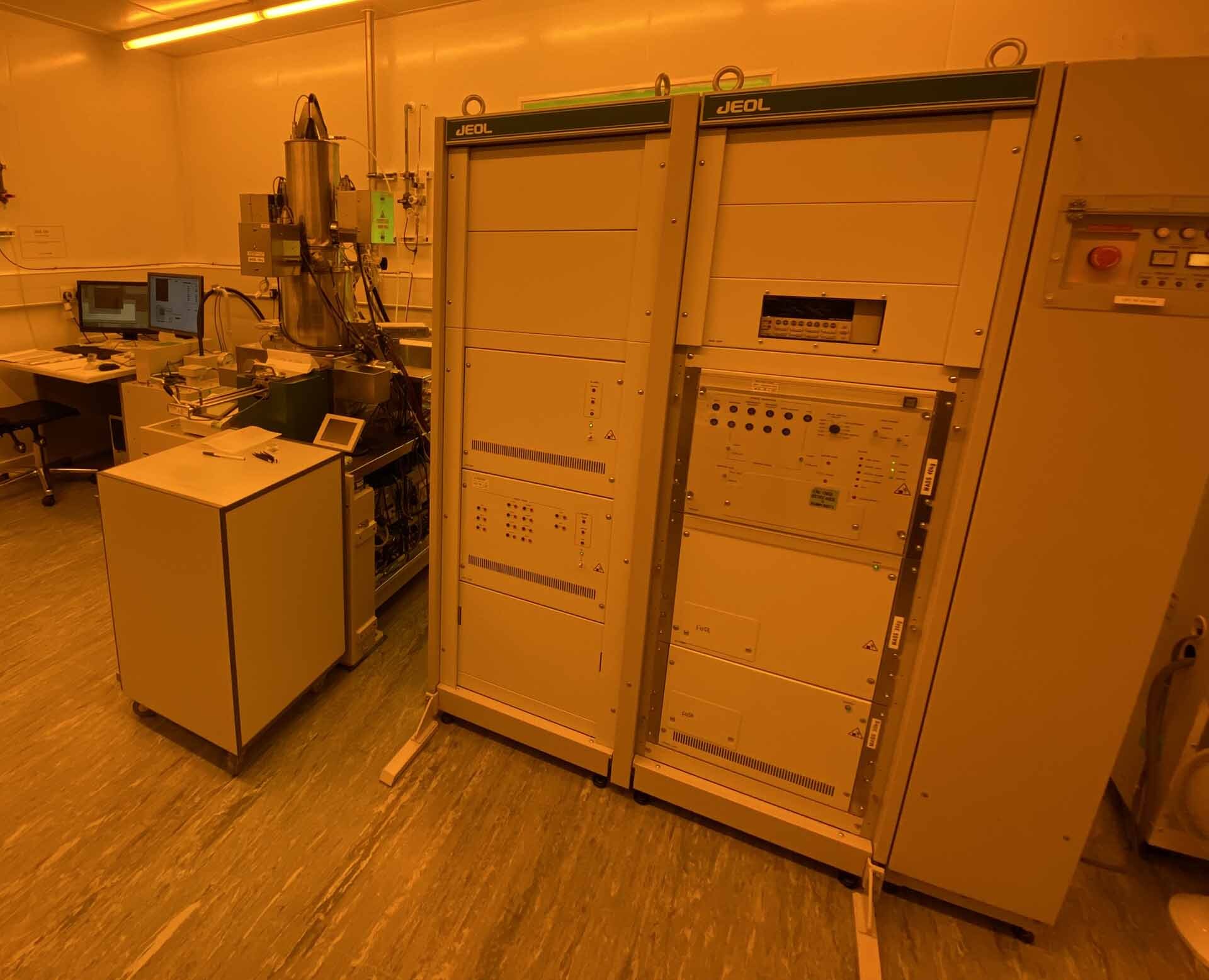
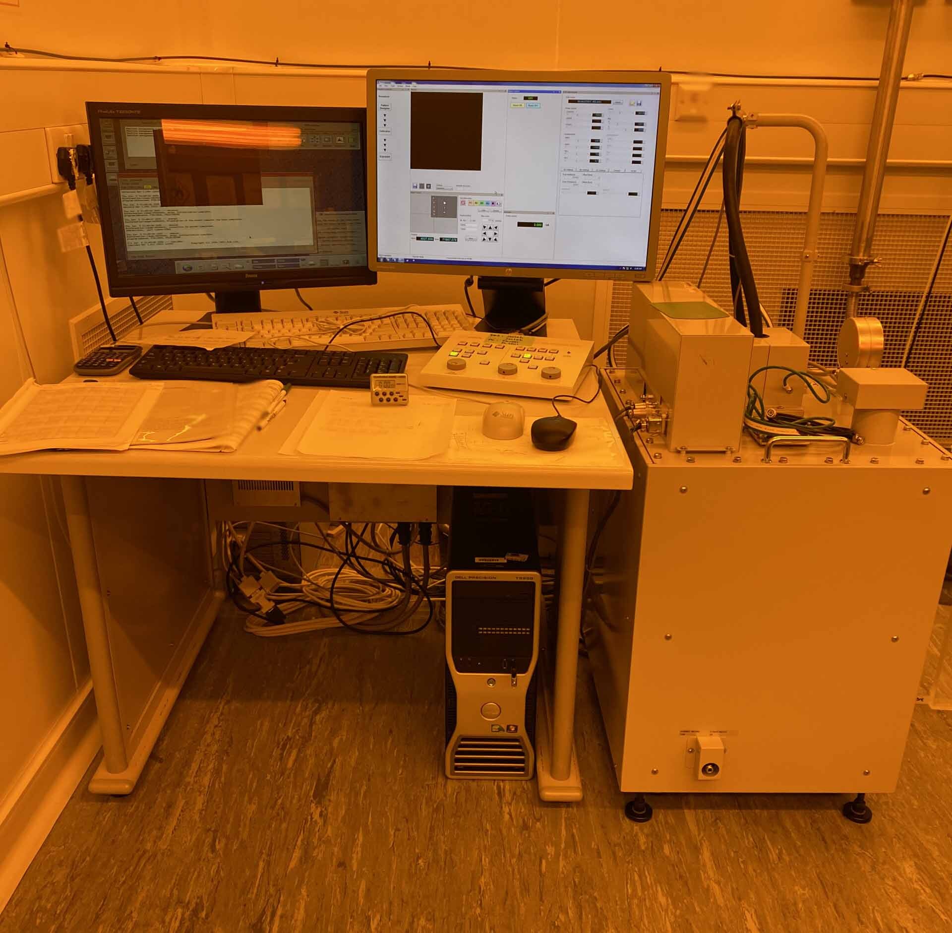
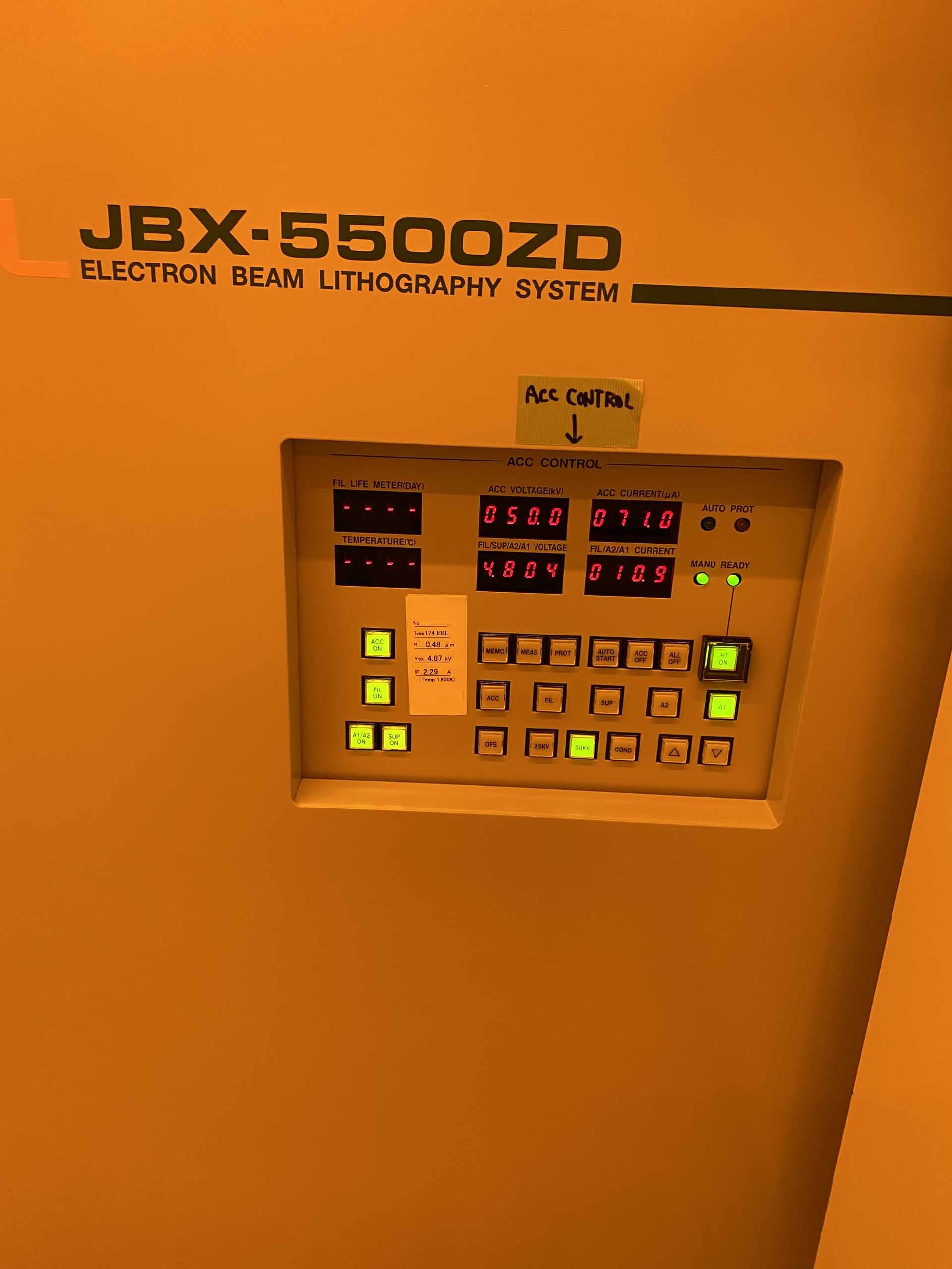
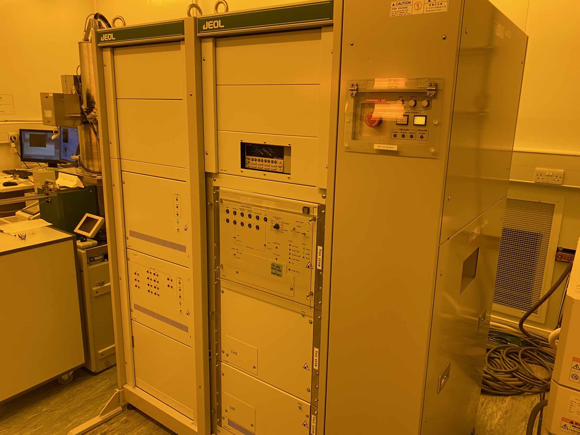
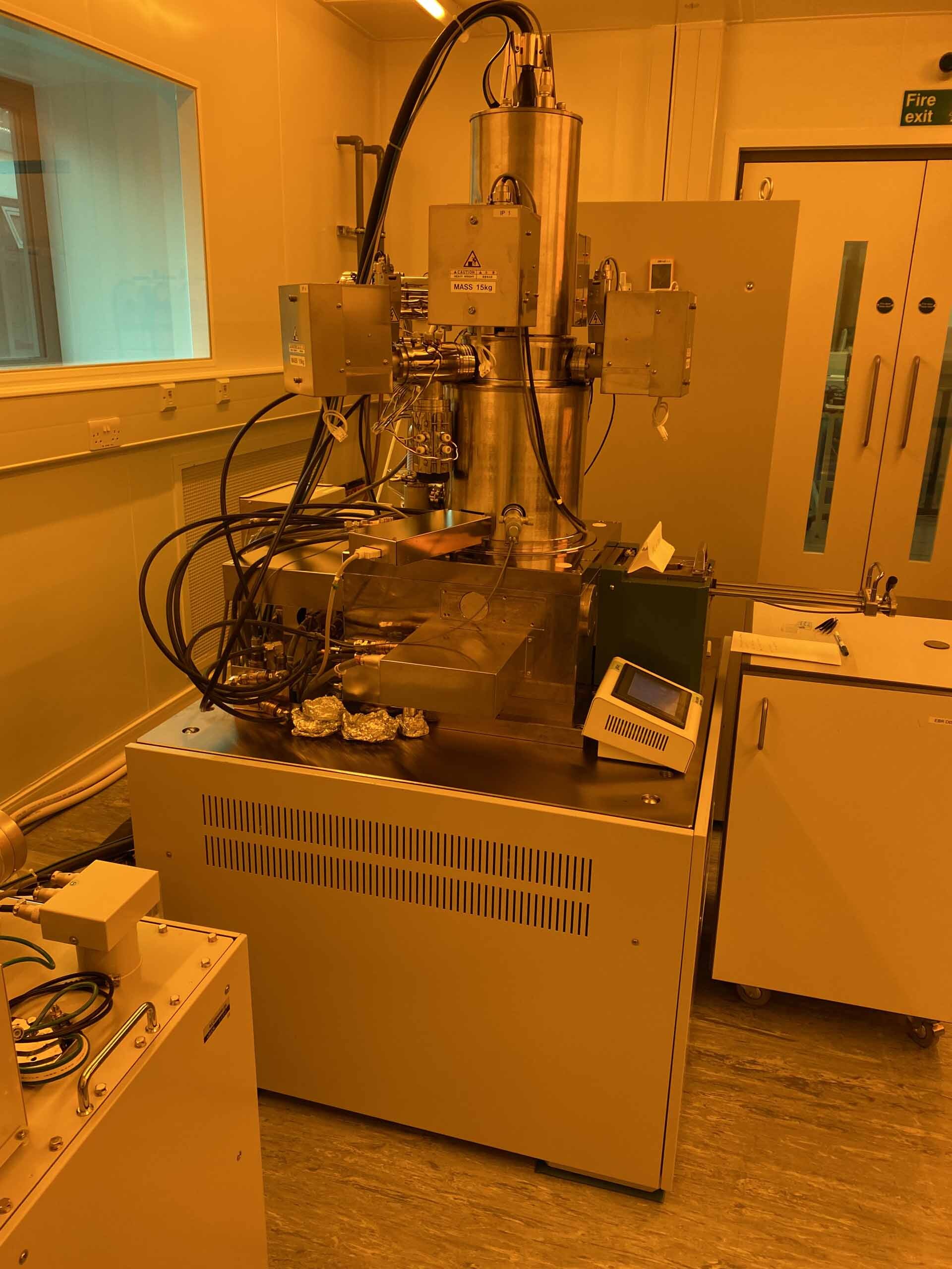
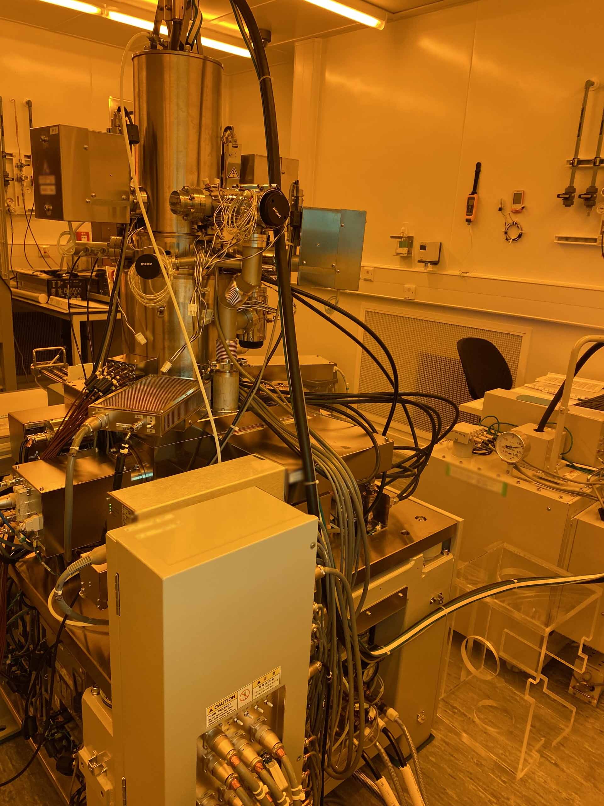
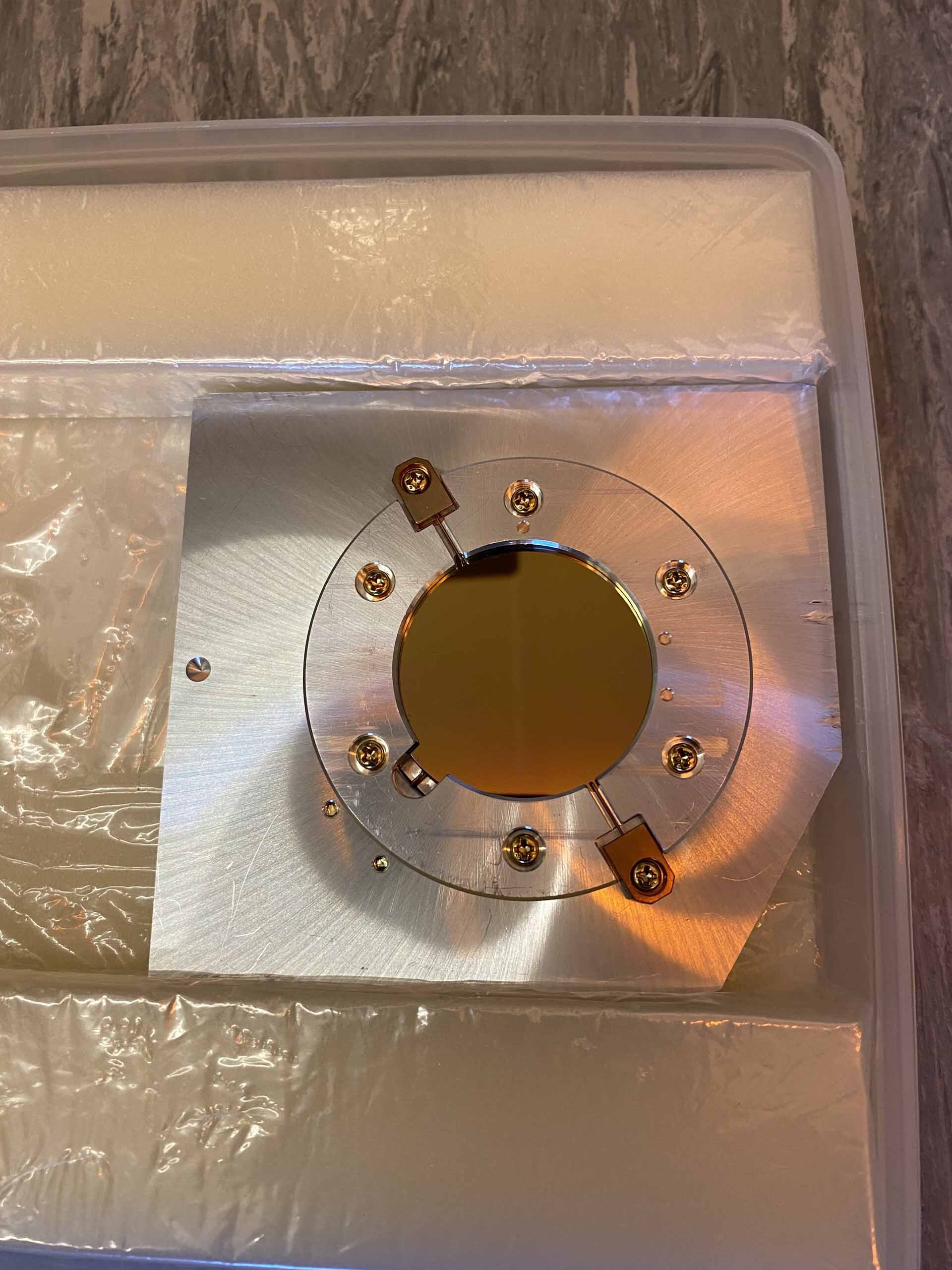
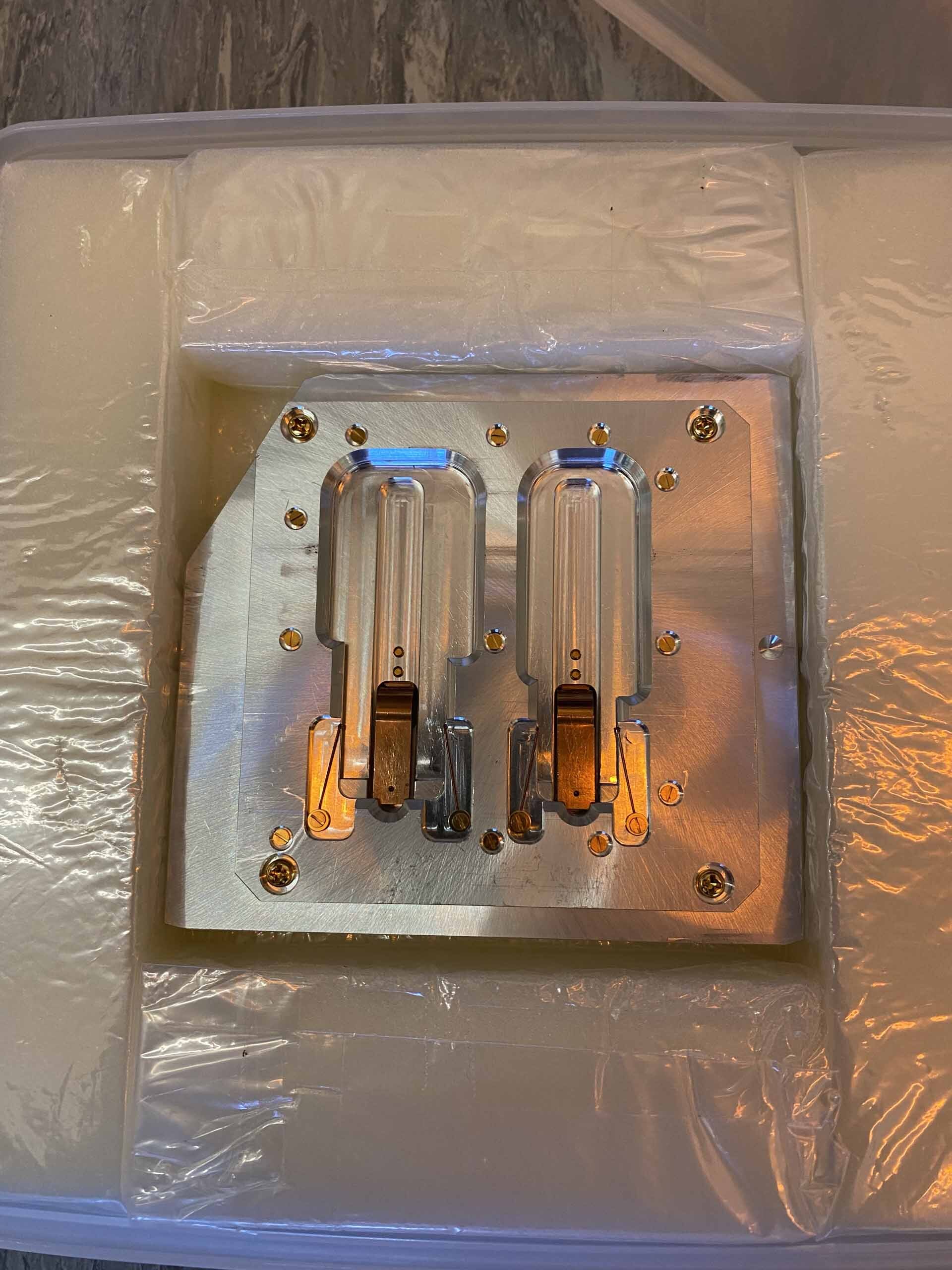
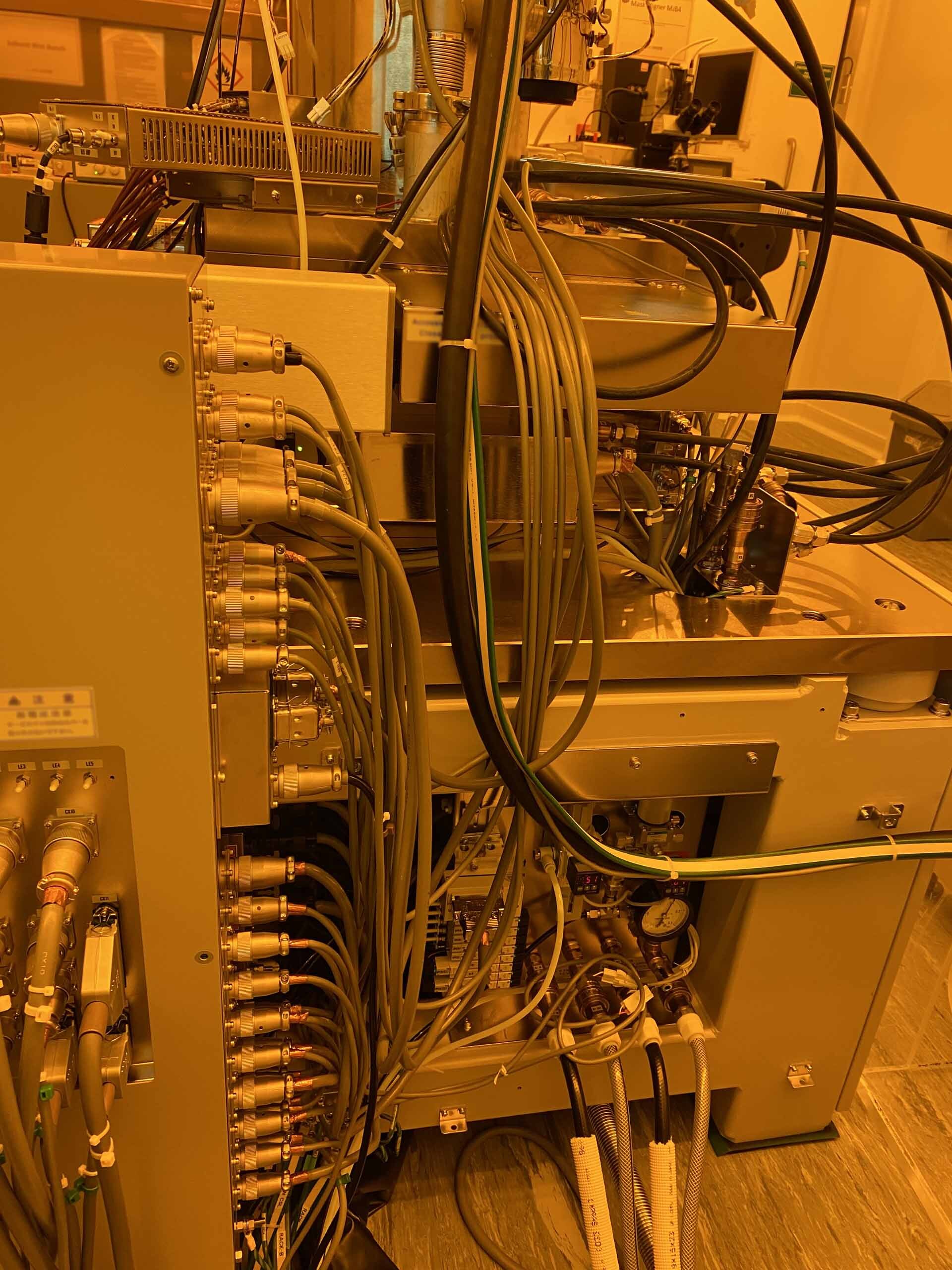
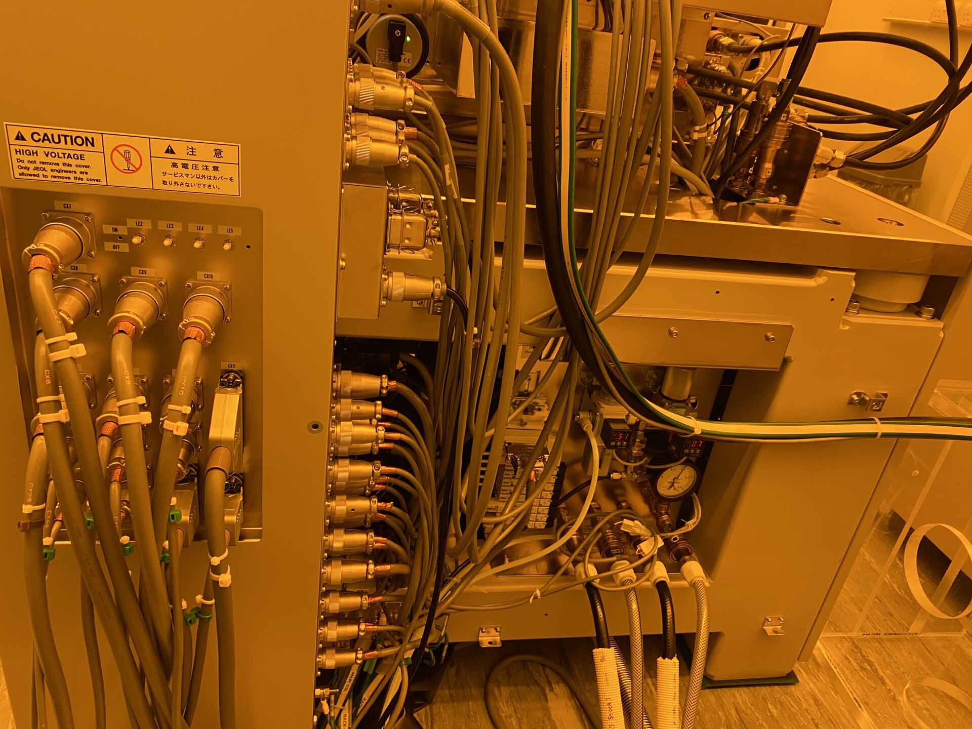
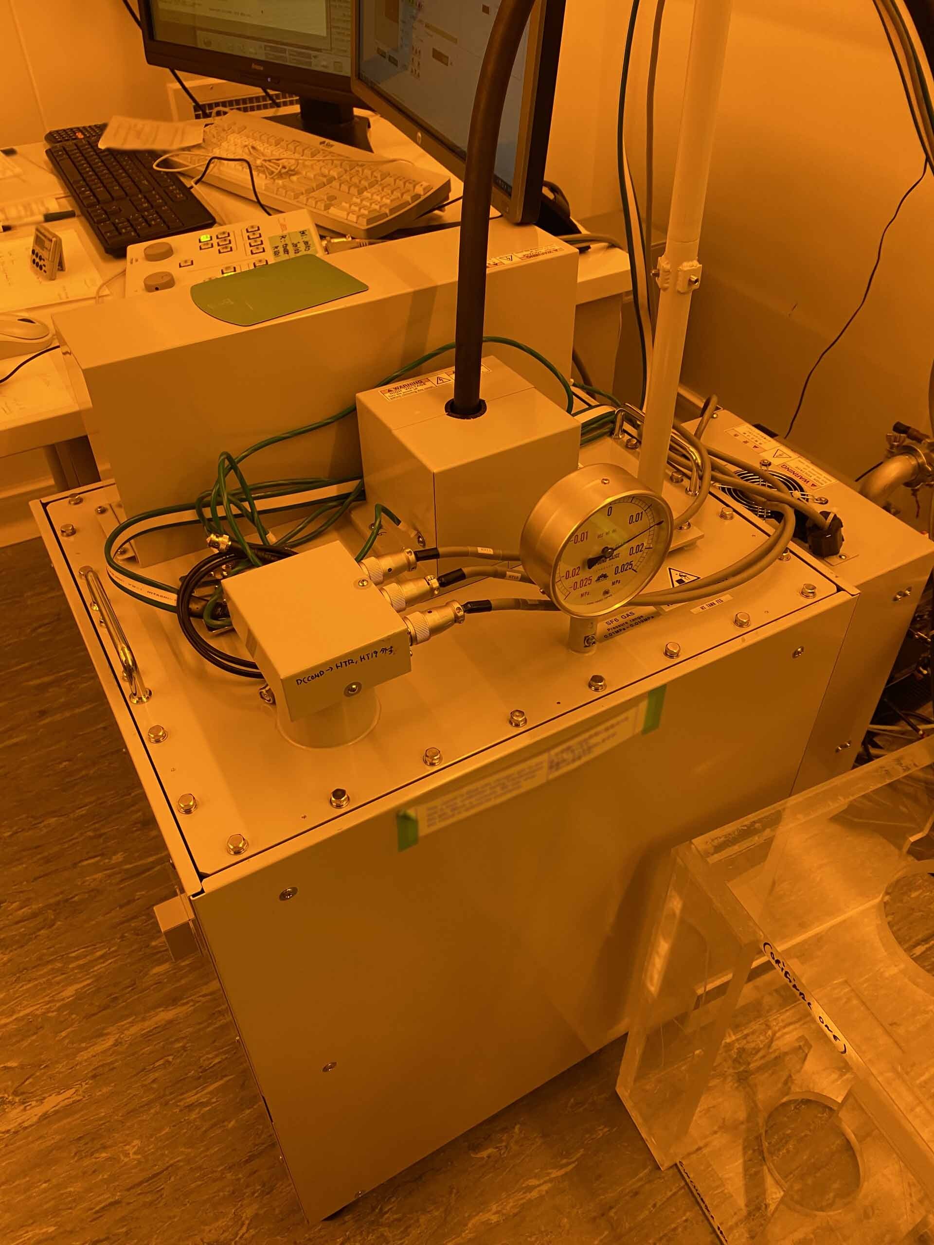
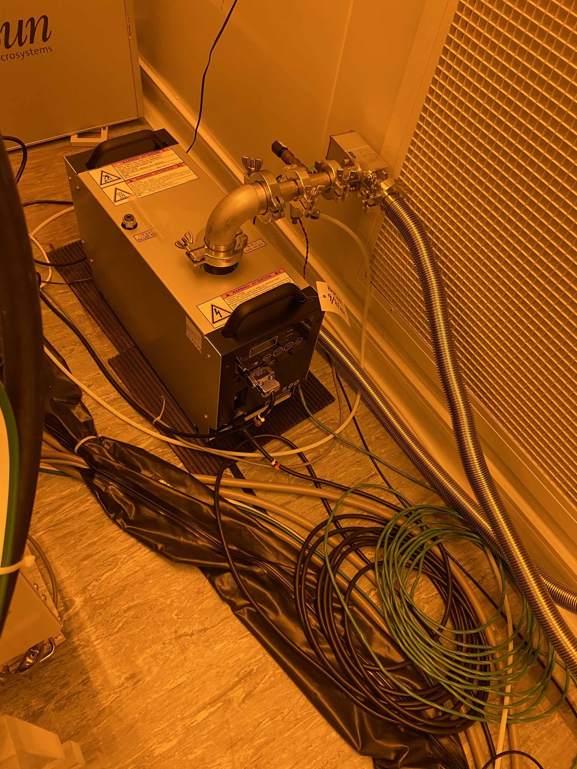
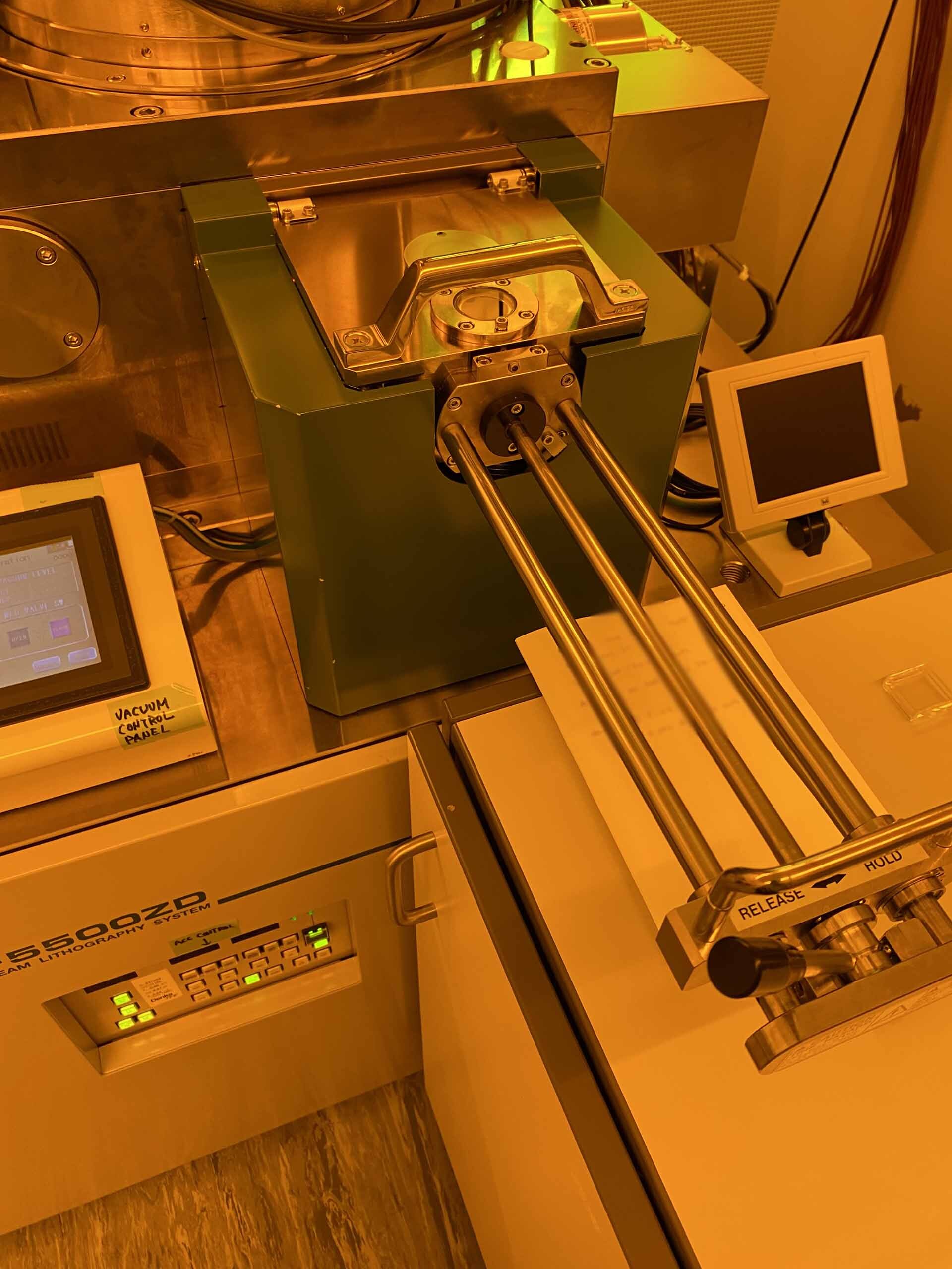
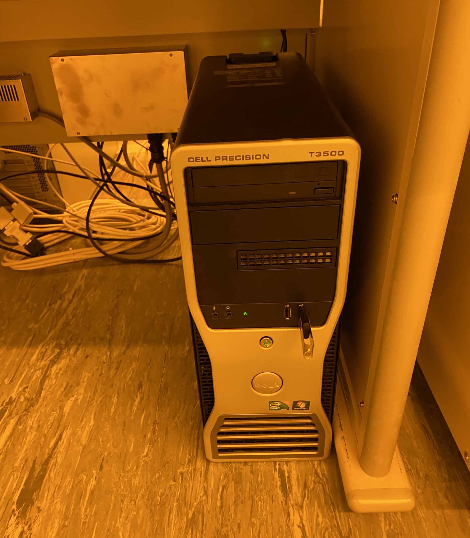
ID: 293775451
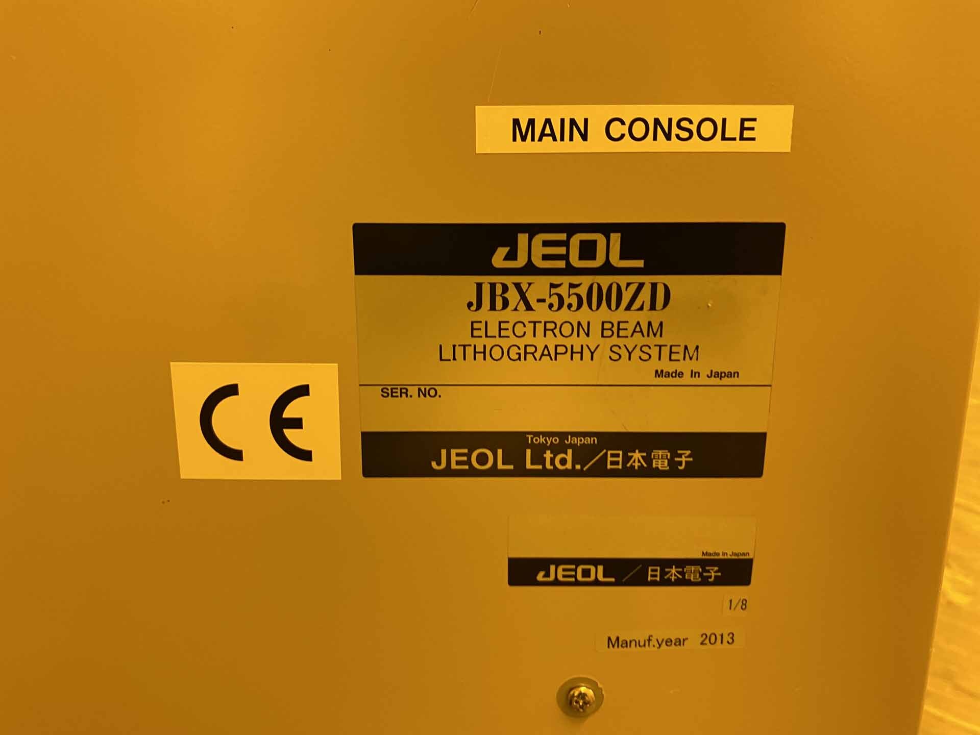
Vintage: 2013
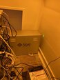
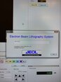
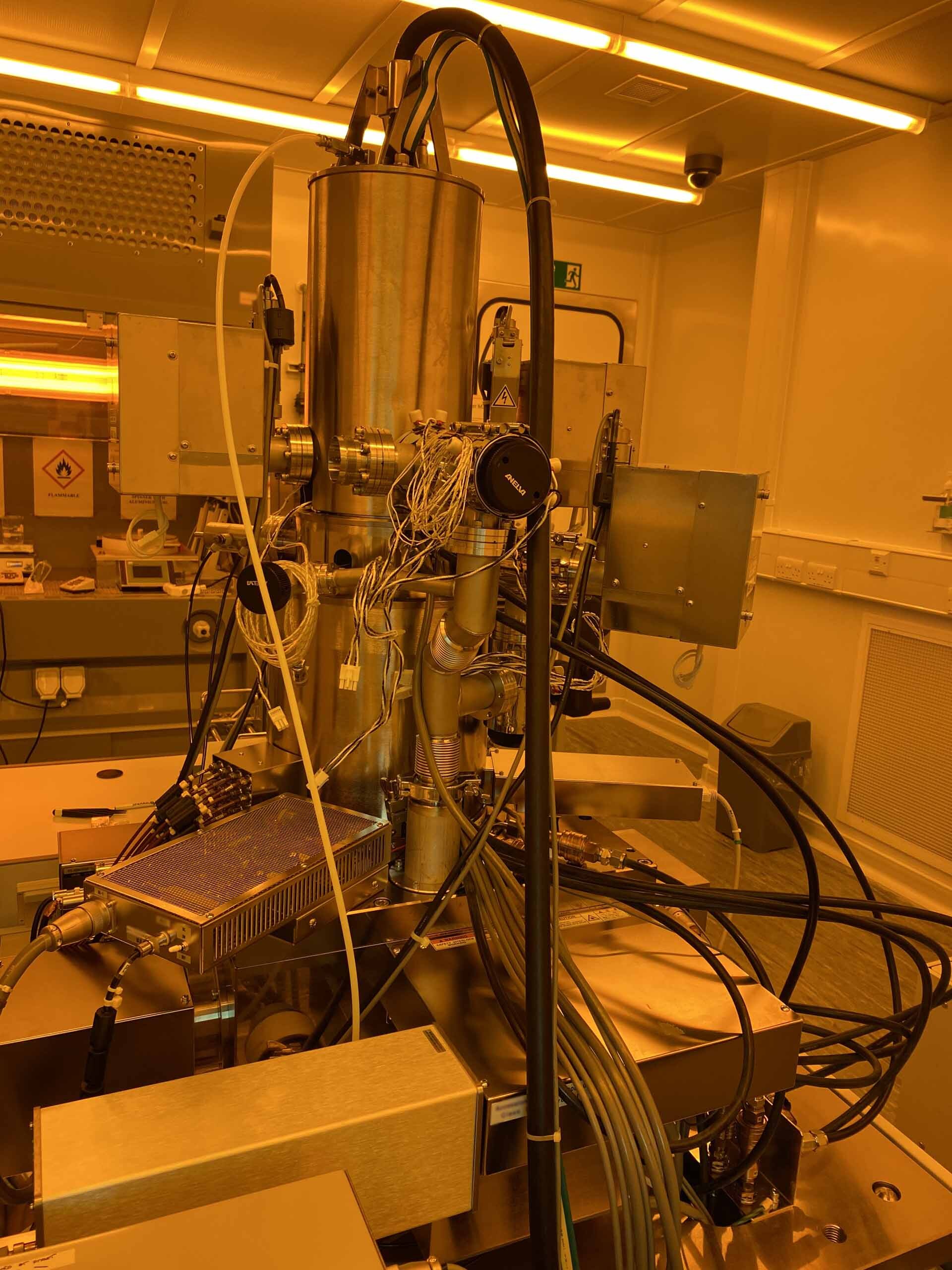
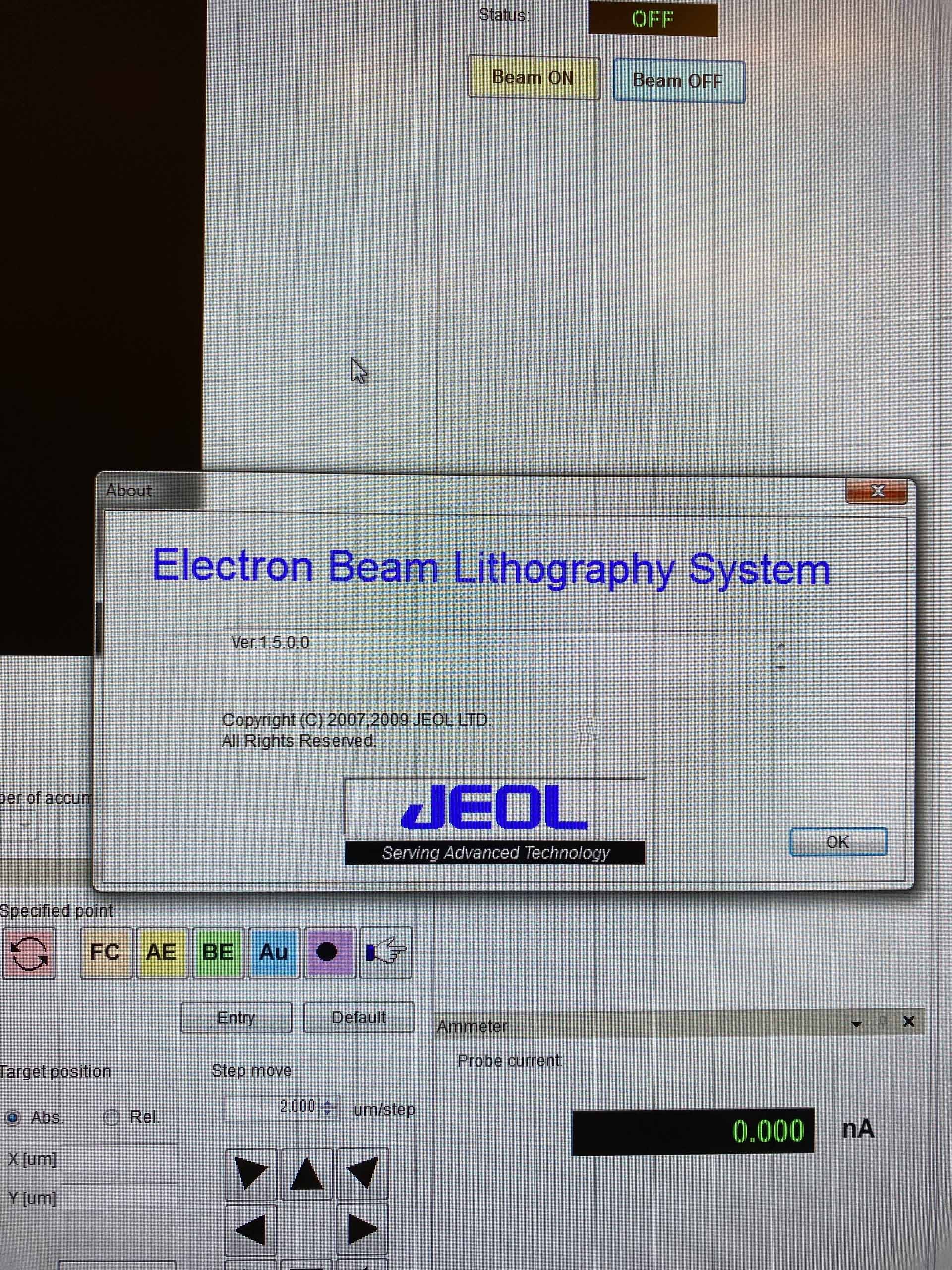
E-Beam lithography system
Electron emitter: TFE (ZrO/W)
Acceleration voltage: 50 keV
Beam current: 30 pA - 20 nA
Field size: 100 µm, 1000 µm
Beam scanning speed: 12 MHz
Manual loader
Wafer holder, 4"
XY Stage
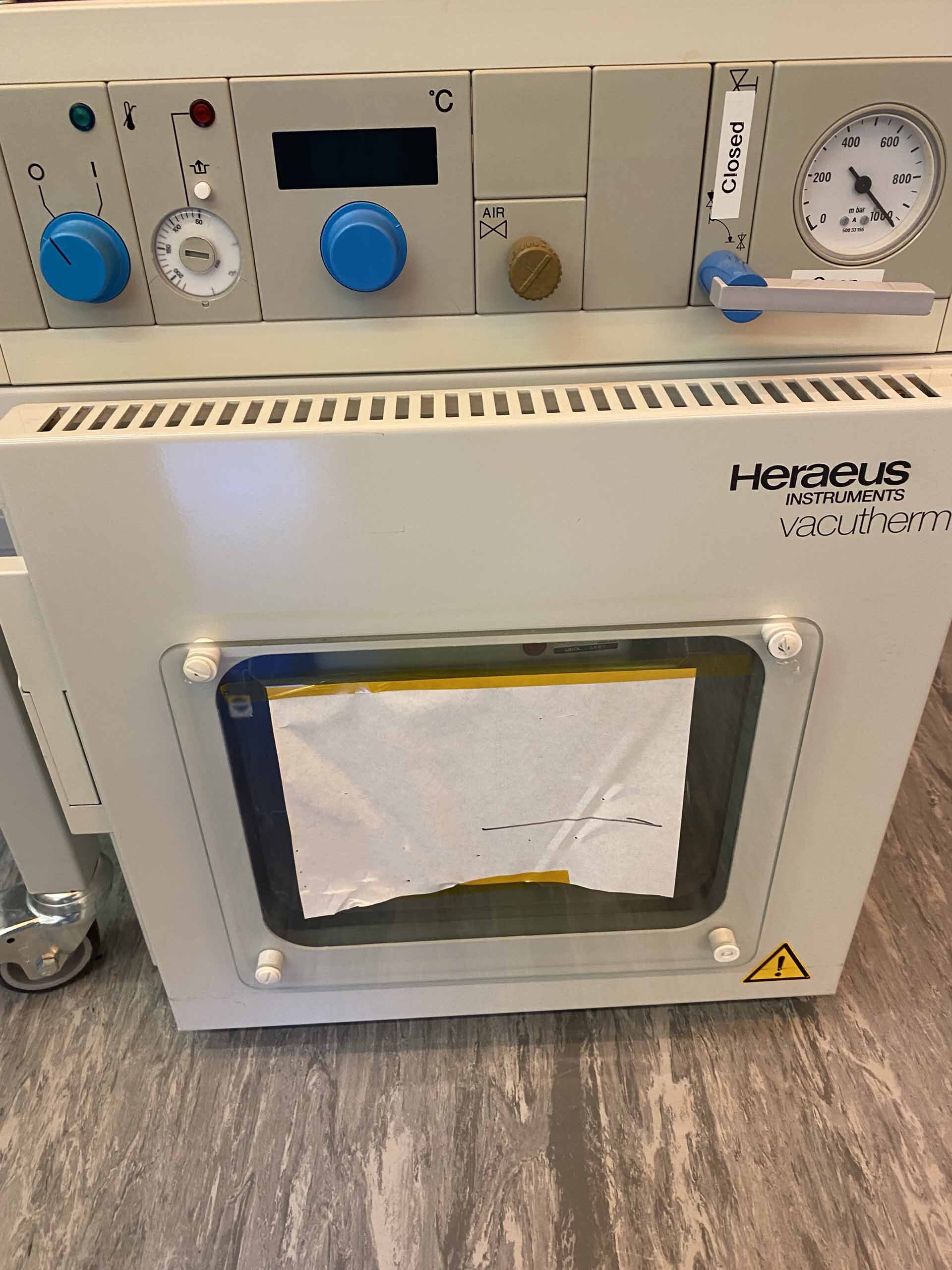
Dry pump
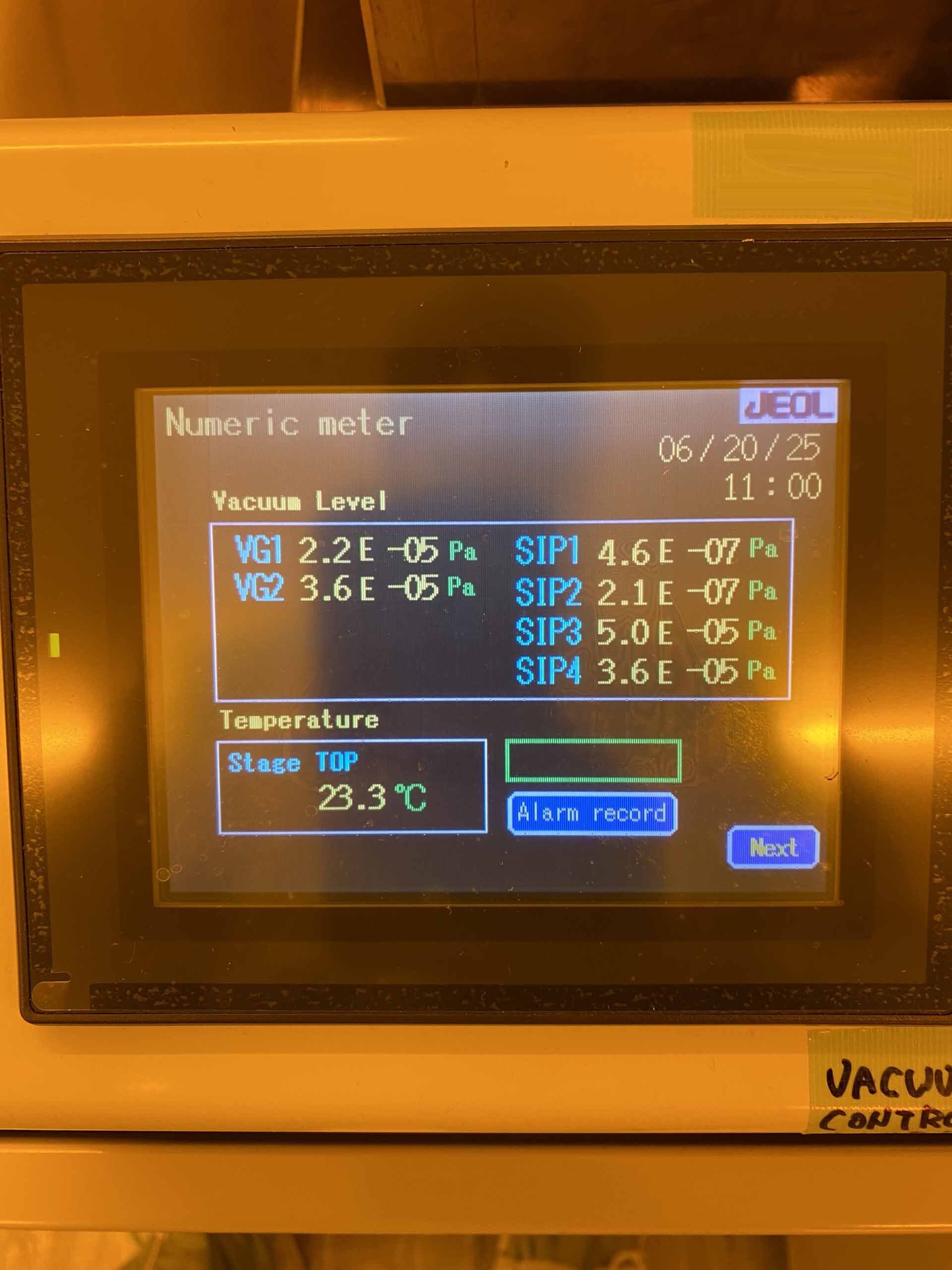
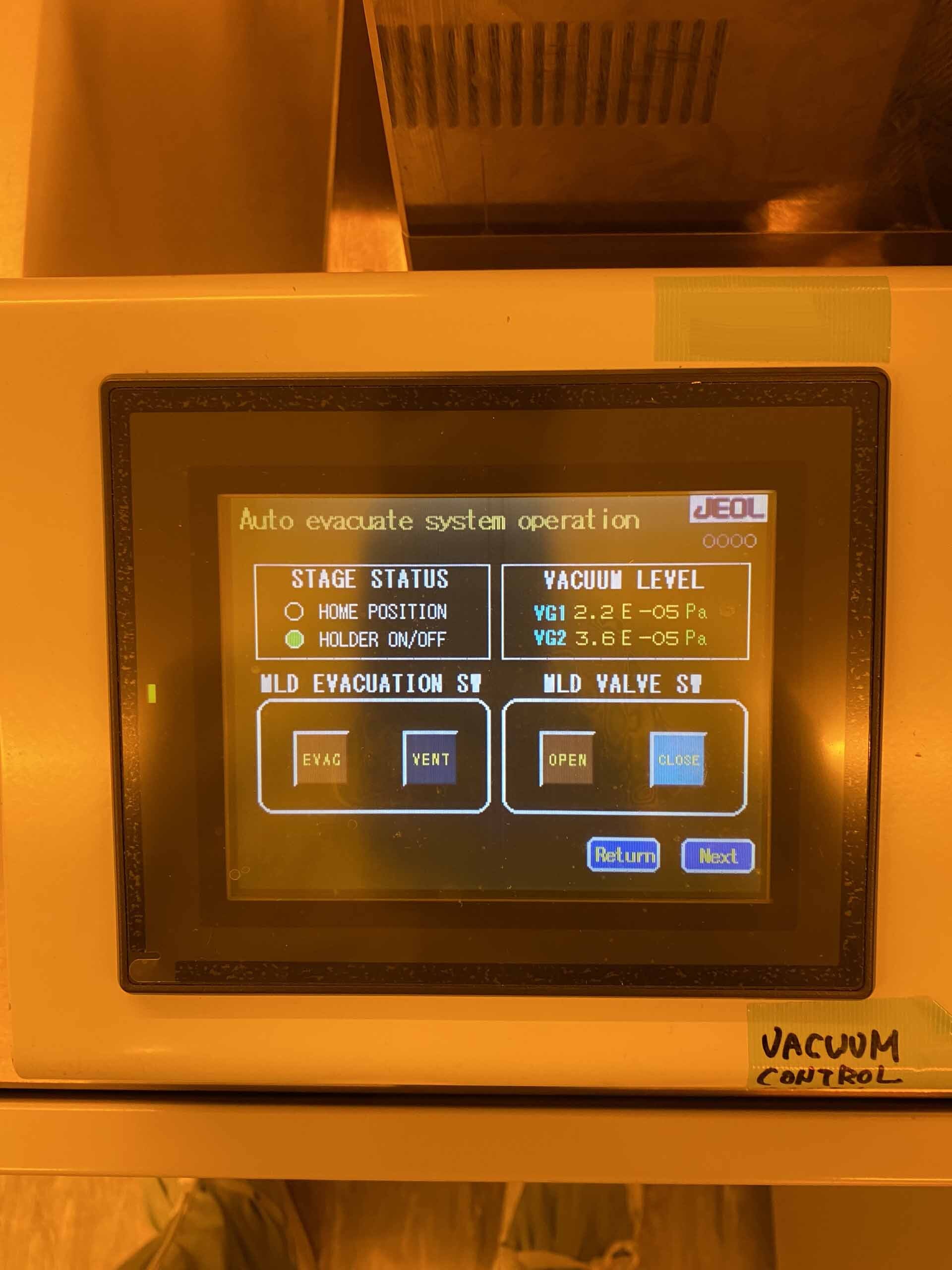
Vacuum pump
Valves
Clean Dry Air (CDA)
Beam shape: Circular spot
Gas: SF6
Stage movement: 104 x 75 mm
Emitter non-functional
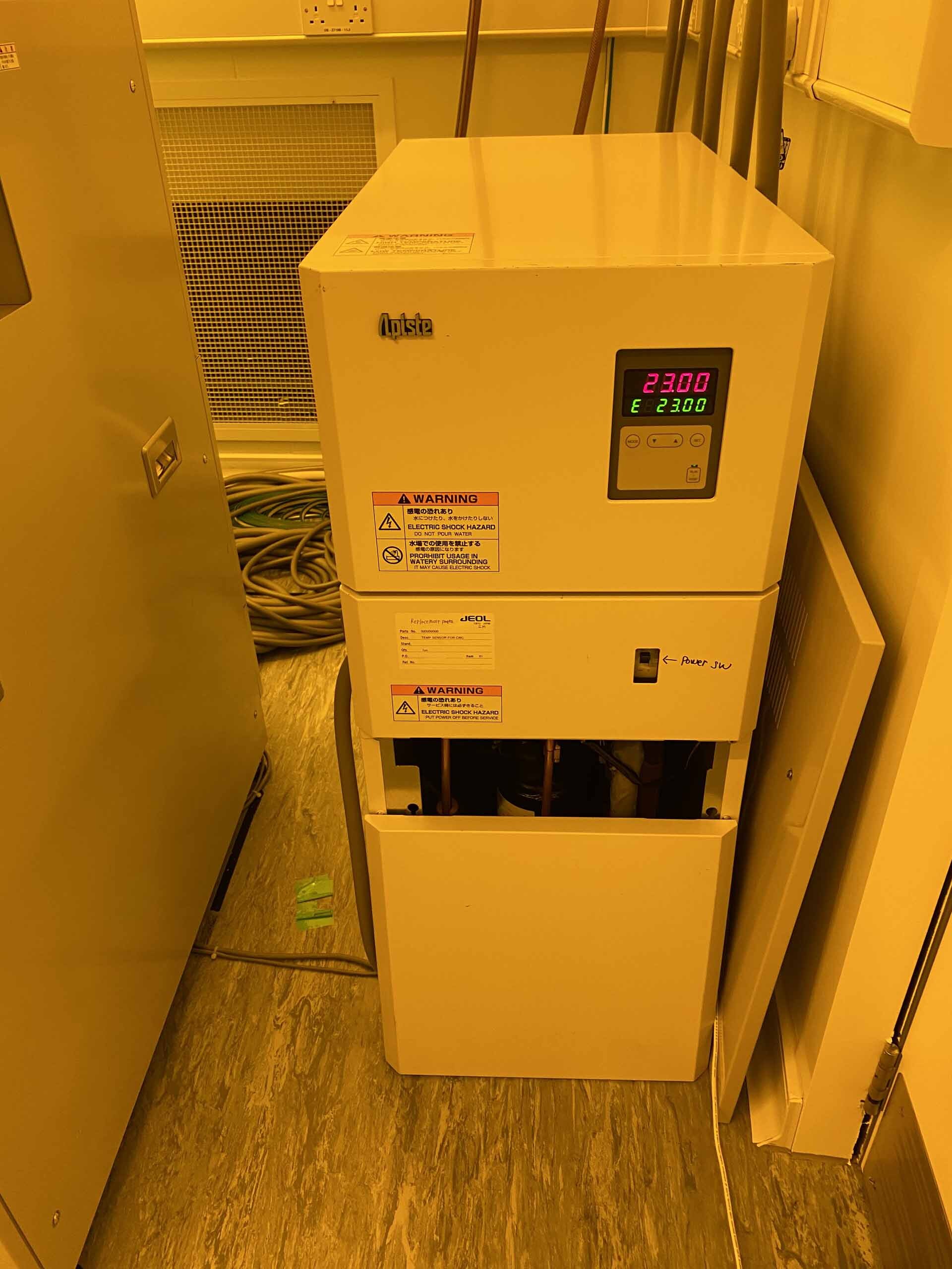
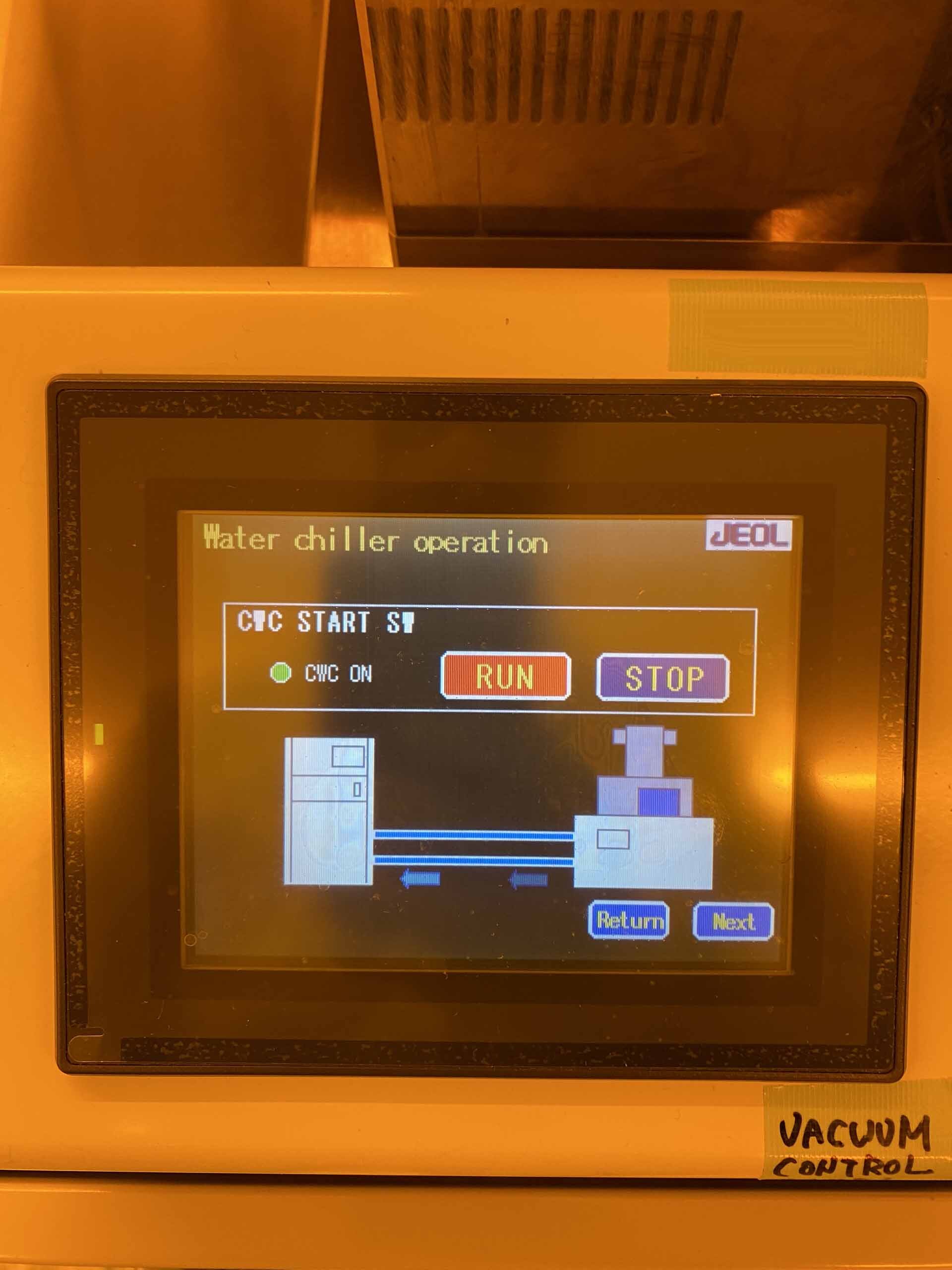
Cooling water system:
Flow rate: 6 L/min
Pressure: 0.15 to 0.5 MPa
Temperature: 15° to 32°C
Writing modes:
Accelerating voltage / Objective lens / Maximum write field size / Minimum E-Beam size
25 kV / 4th Lens / 2000 x 2000 µm² / 10 nm
50 kV / 4th Lens / 1000 x 1000 µm² / 5 nm
25 kV / 5th Lens / 200 x 200 µm² / 1 nm
50 kV / 5th Lens / 100 x 100 µm² / 0.5 nm
(3) Cassettes:
BX-Z12016TMPC/S
BX-Z12017TMPC/S
BX-Z0714507W2T
Liquid crystal display
Hard Disk Drive (HDD)
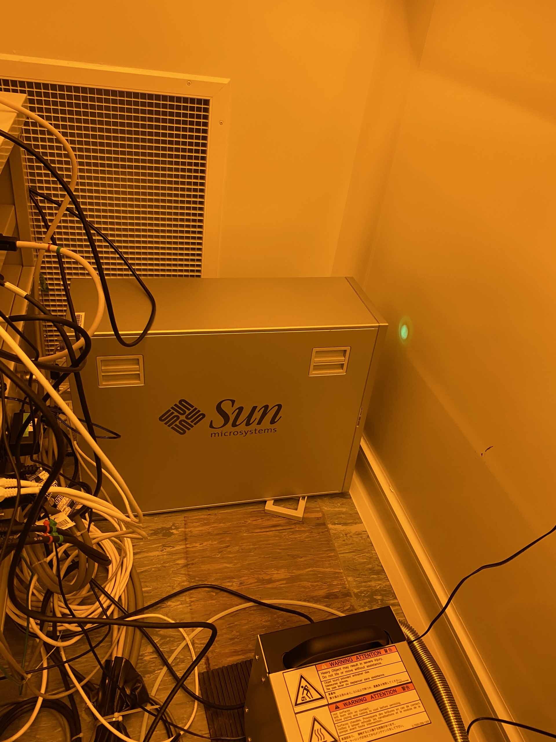
Workstation
PC
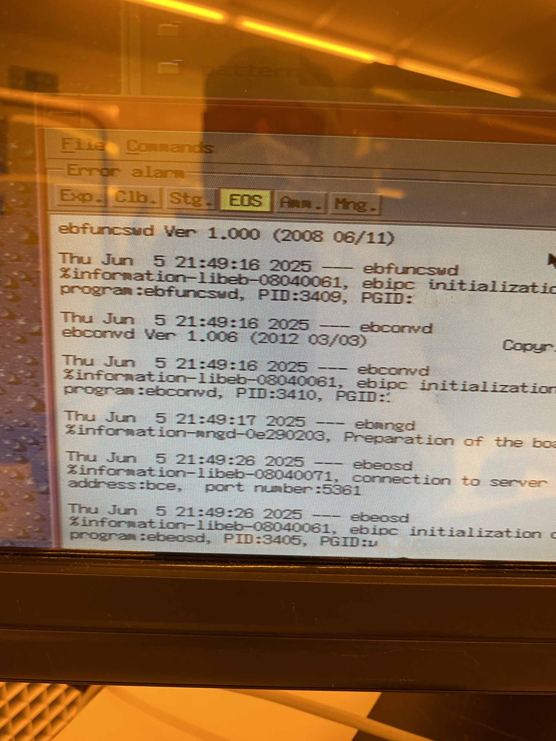
Operating system: Windows XP
Manuals included
Power supply: 100-200 VAC, 50/60 Hz
2013 vintage.
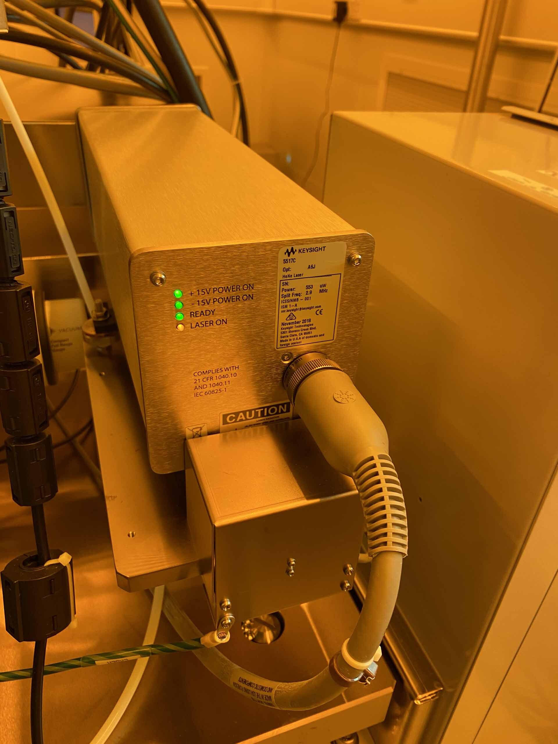
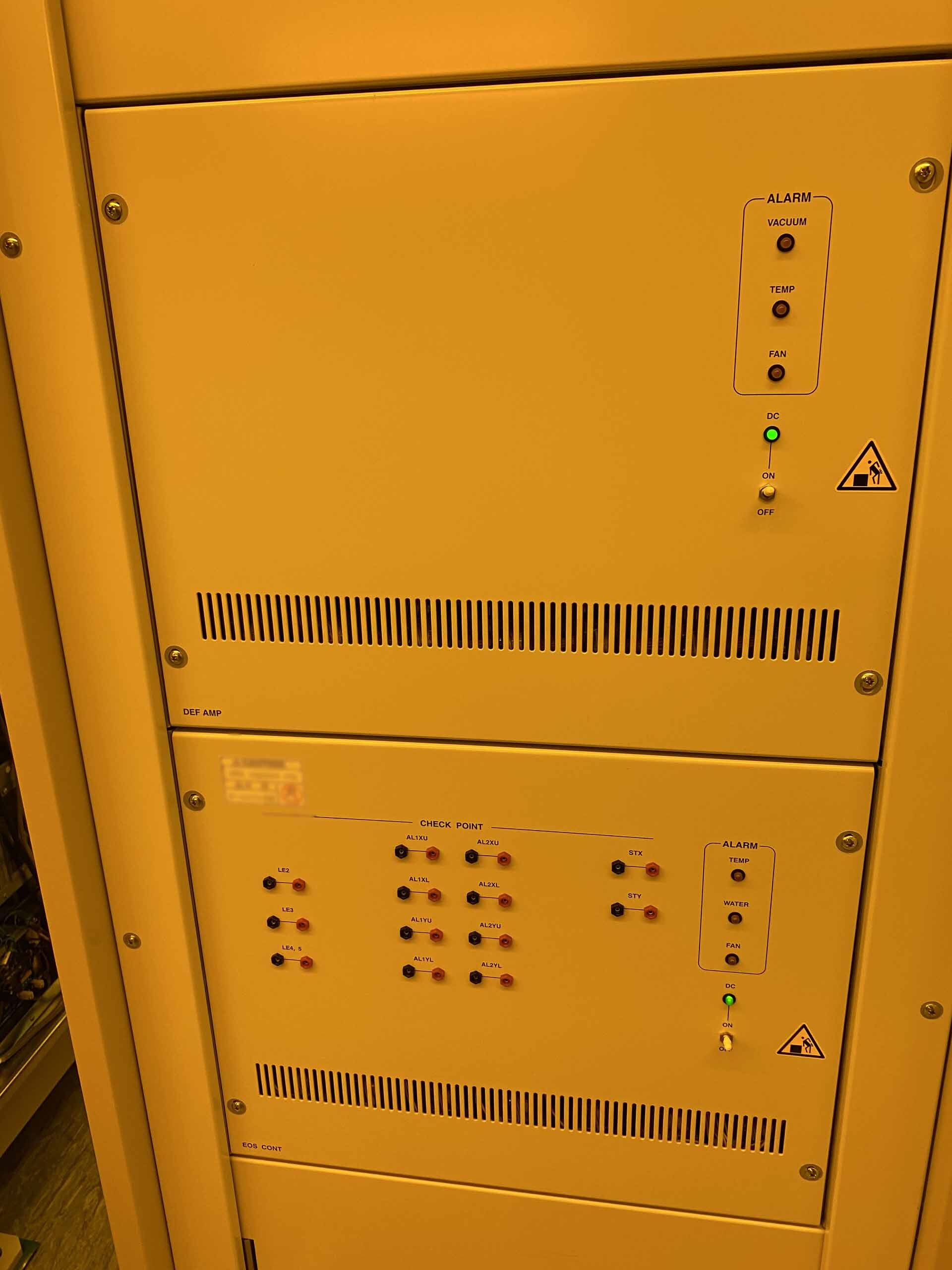
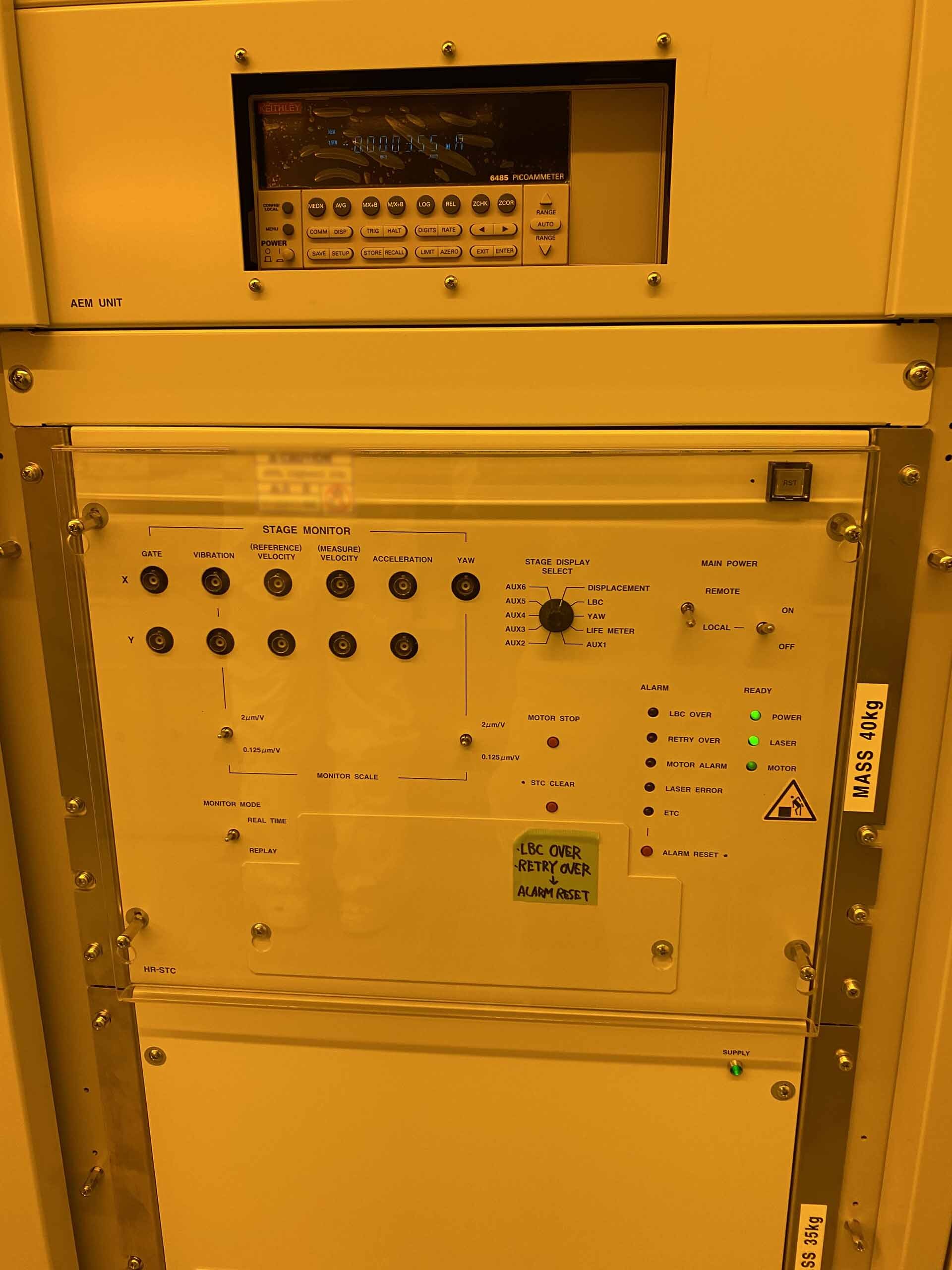
JEOL JBX-5500FS is a cutting-edge scanning electron microscope (SEM) that sets a new standard in high-resolution imaging, precise patterning, and advanced nanofabrication capabilities. This instrument is designed for a diverse range of applications in materials science, semiconductor research, bioengineering, and nanotechnology. At the heart of JEOL JBX-5500 FS is its electron optics equipment, which incorporates a field emission electron gun capable of producing a highly focused electron beam with sub-nanometer resolution. This enables the microscope to achieve exceptional imaging performance, capturing detailed surface topography and ultrafine structures with remarkable clarity and precision. The high-brightness electron source also allows for enhanced signal detection and sensitivity, making it ideal for imaging samples with low contrast or low atomic number elements. One of the key features of JBX-5500FS is its versatile patterning capability, which is achieved through the use of a high-precision electron beam lithography system. This feature enables researchers to create custom-designed nanostructures and patterns on a variety of substrates with sub-10 nm resolution. The instrument supports a wide range of lithography modes, including direct write, proximity, and projection lithography, giving users the flexibility to tailor their patterning approach to suit their specific needs. Thanks to its advanced automation and control systems, JBX-5500 FS offers a user-friendly interface that streamlines operation and ensures reproducibility in experimental procedures. The microscope is equipped with sophisticated software tools for image acquisition, analysis, and data processing, allowing users to quickly generate high-quality images and obtain valuable insights into their samples. Moreover, the unit's intuitive programming capabilities enable complex lithography patterns to be created with ease, facilitating rapid prototyping and efficient device fabrication. In terms of nanofabrication capabilities, JEOL JBX-5500FS excels in producing intricate nanostructures with high aspect ratios and precise dimensions. The machine can deposit and etch a variety of materials, including metals, polymers, and oxides, enabling researchers to create complex three-dimensional structures for a wide range of applications. Additionally, the microscope supports in-situ monitoring and real-time feedback during fabrication processes, ensuring accurate control over feature size, shape, and alignment. JEOL JBX-5500 FS is also equipped with an array of advanced imaging and analytical techniques that enhance its versatility and functionality. These include energy-dispersive X-ray spectroscopy (EDS) for elemental analysis, electron backscatter diffraction (EBSD) for crystallographic characterization, and cathodoluminescence (CL) for studying optical properties of materials. By combining these imaging modalities with its high-resolution imaging and lithography capabilities, the microscope provides users with a comprehensive toolset for in-depth sample characterization and manipulation. Overall, JBX-5500FS is a state-of-the-art scanning electron microscope that embodies precision, performance, and versatility. Its advanced electron optics, high-resolution imaging, precise patterning, and sophisticated nanofabrication capabilities make it an indispensable tool for researchers and engineers working in diverse fields of science and technology. Whether investigating nanoscale phenomena, fabricating custom nanostructures, or characterizing advanced materials, JBX-5500 FS delivers unparalleled imaging quality and analytical power to drive innovation and discovery in the nanosciences.
There are no reviews yet