Used JEOL JSM 5900LV #293743791 for sale
URL successfully copied!

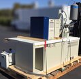

Tap to zoom
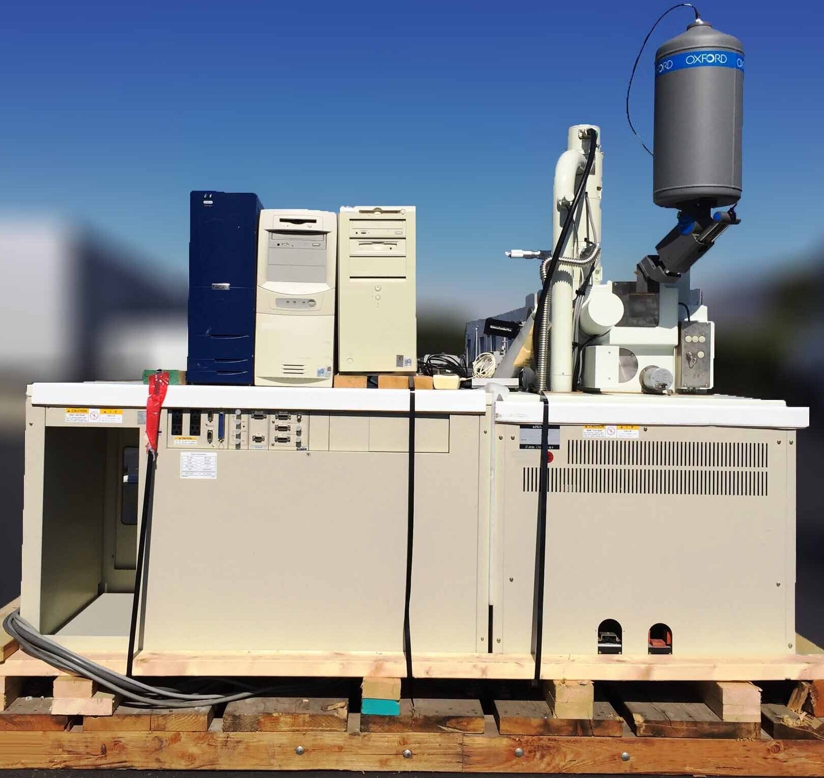

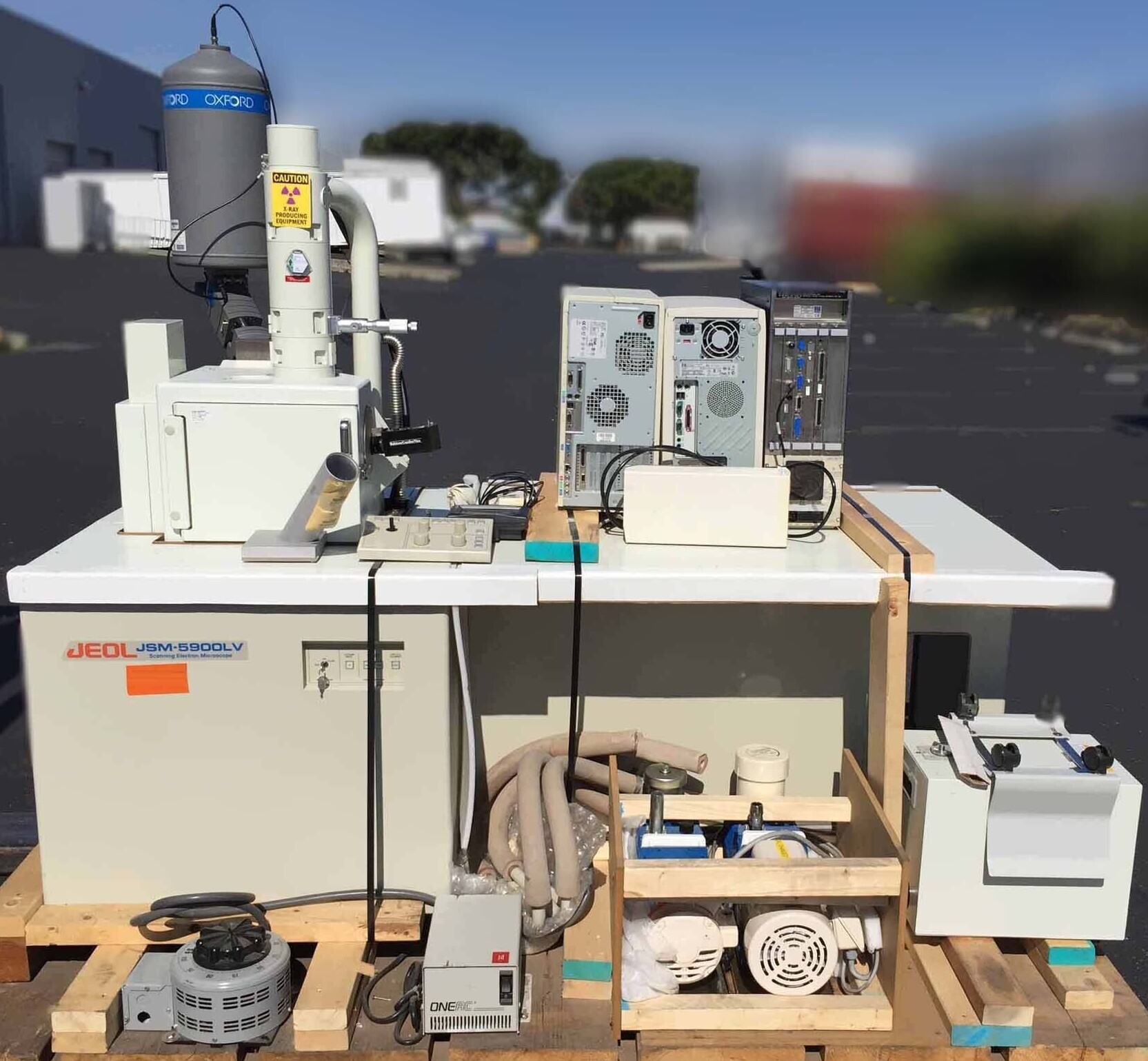
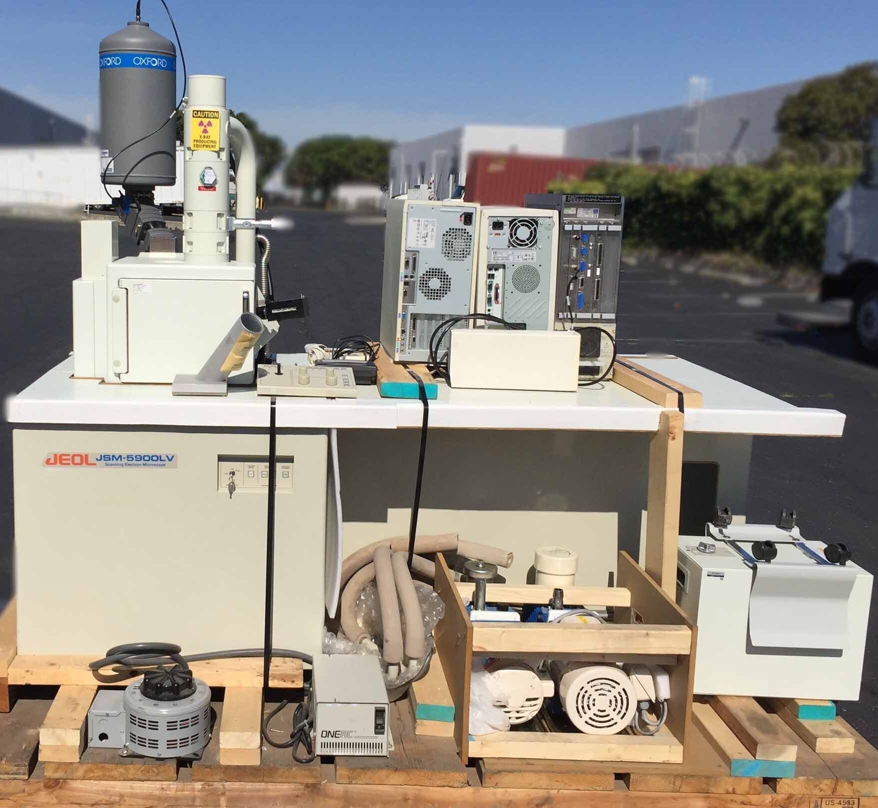
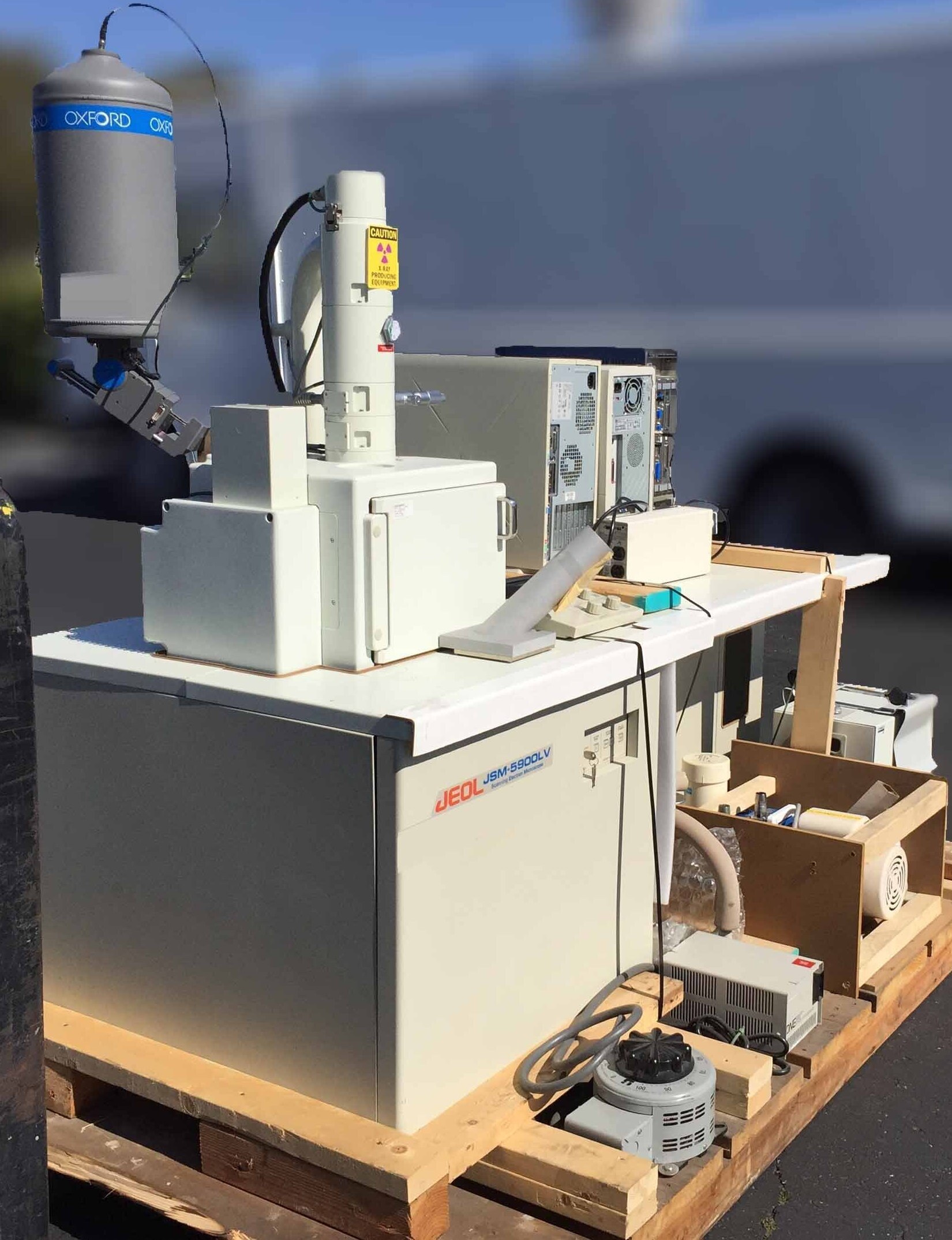
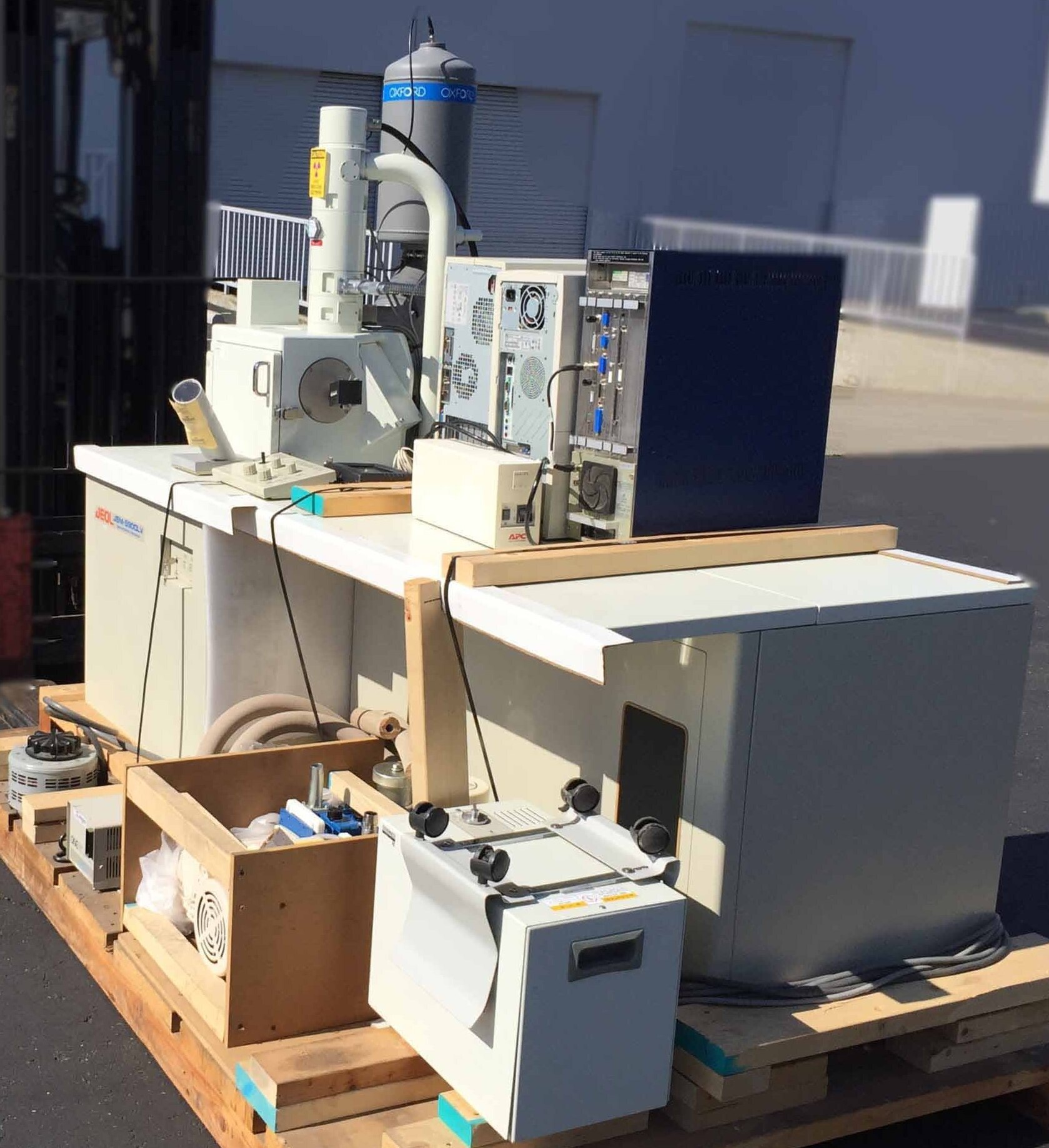
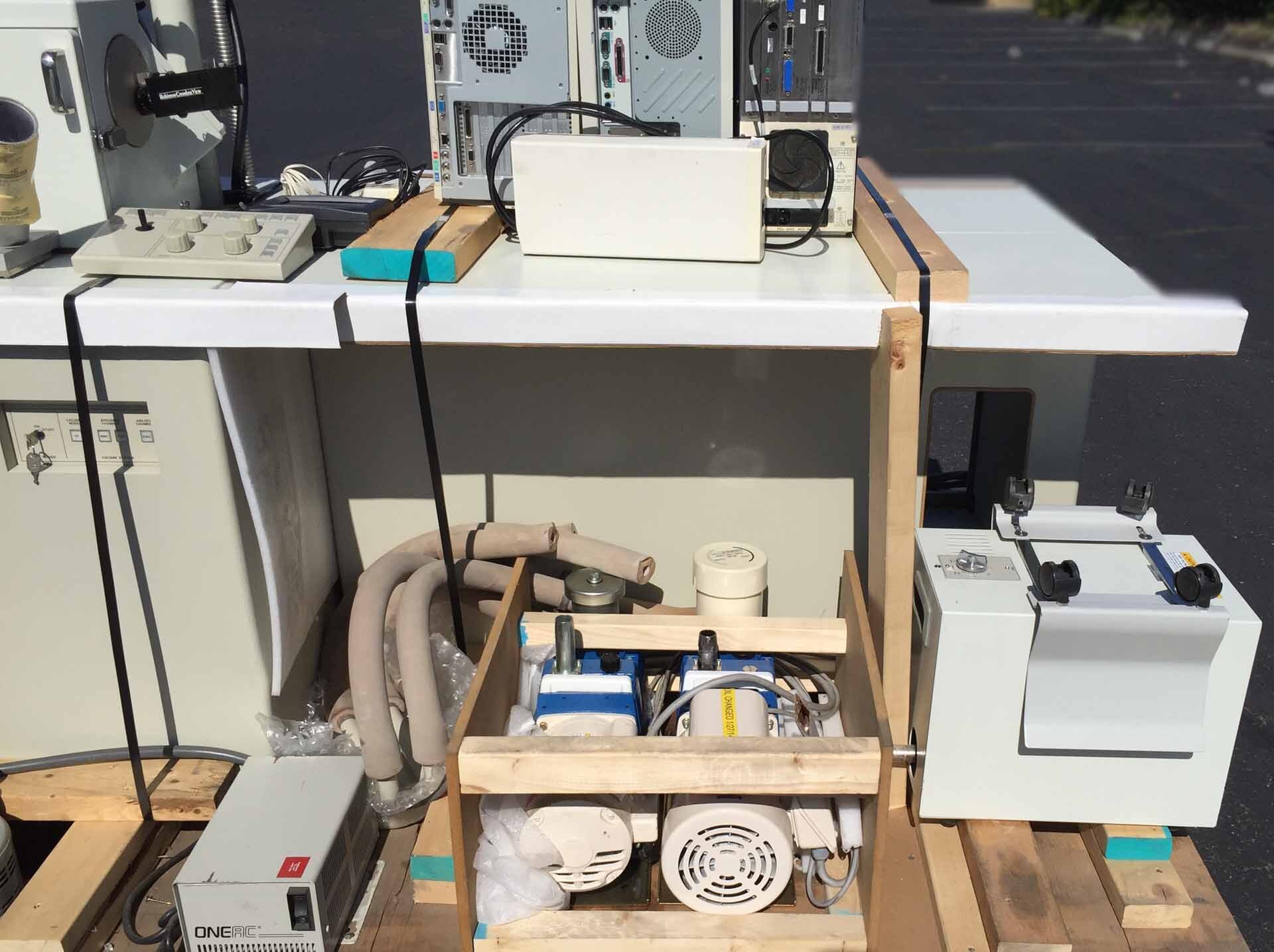
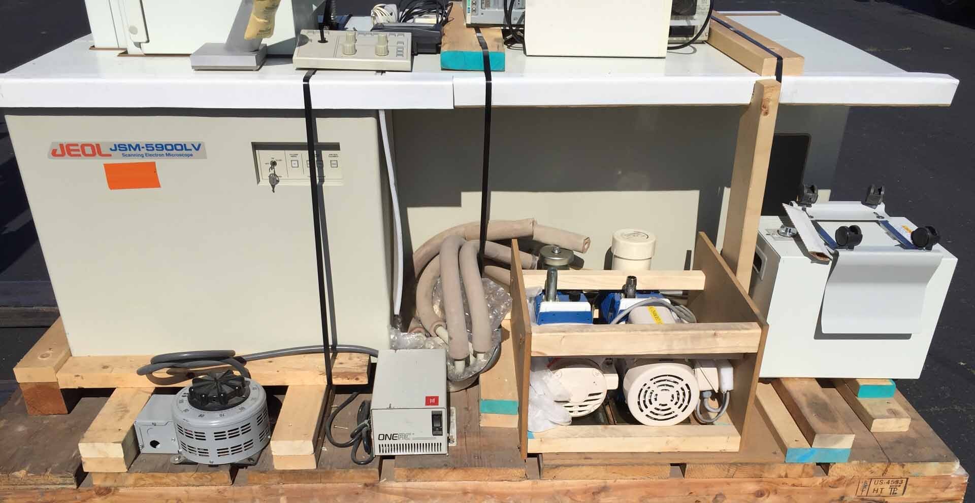
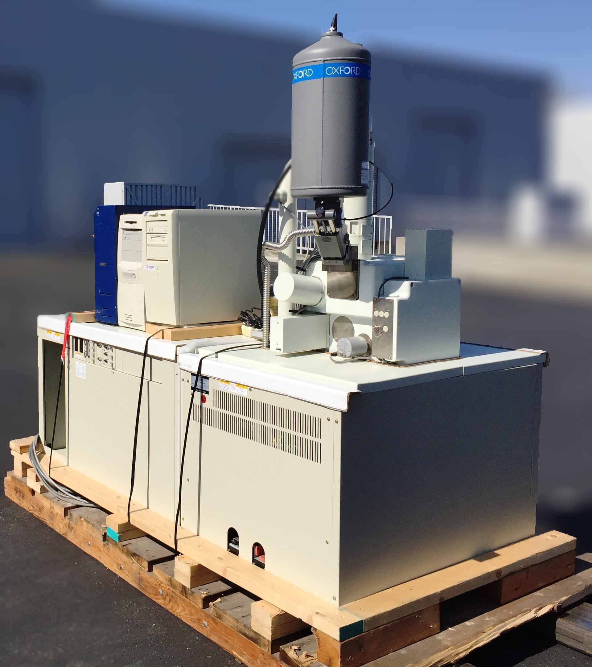
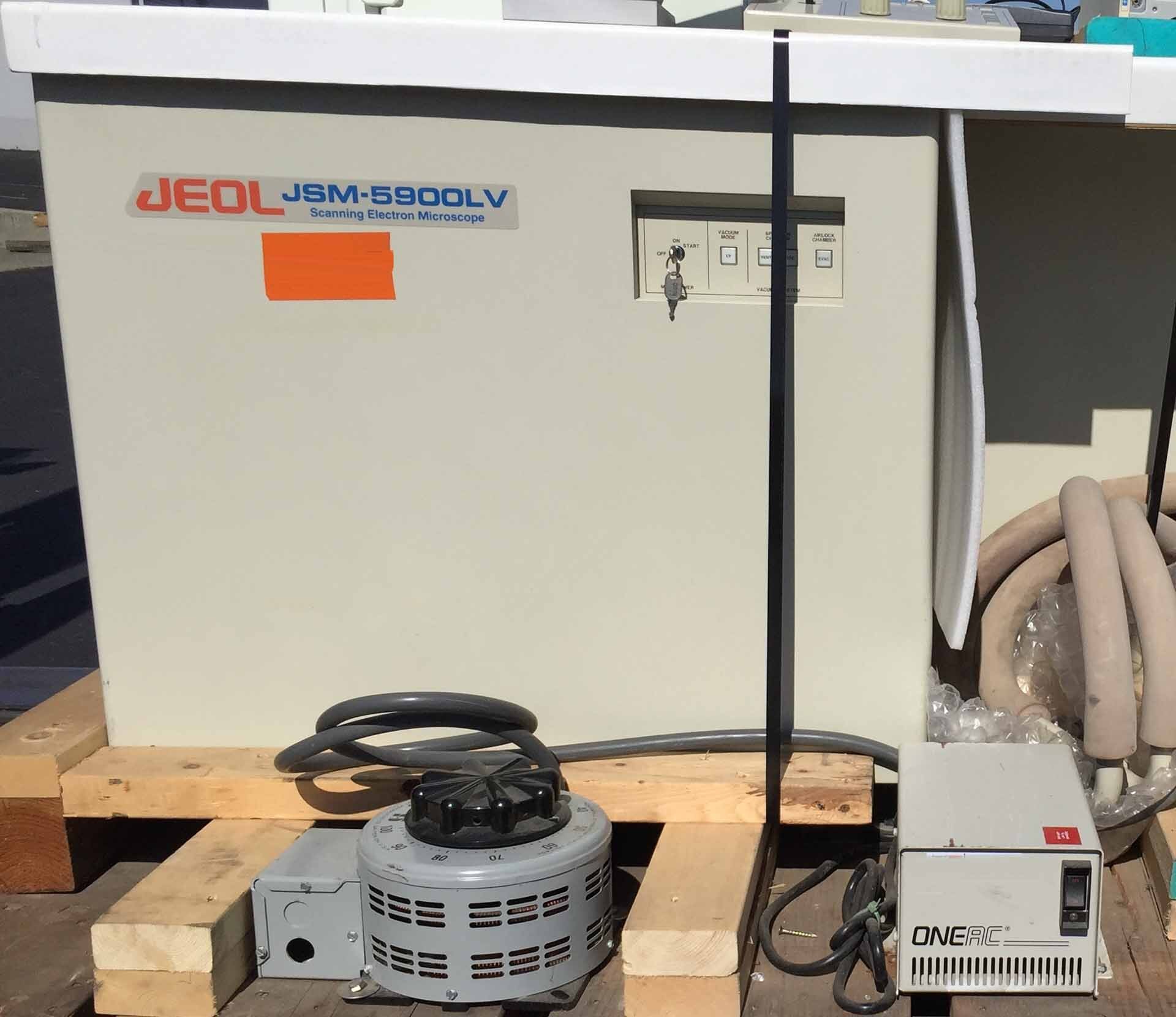
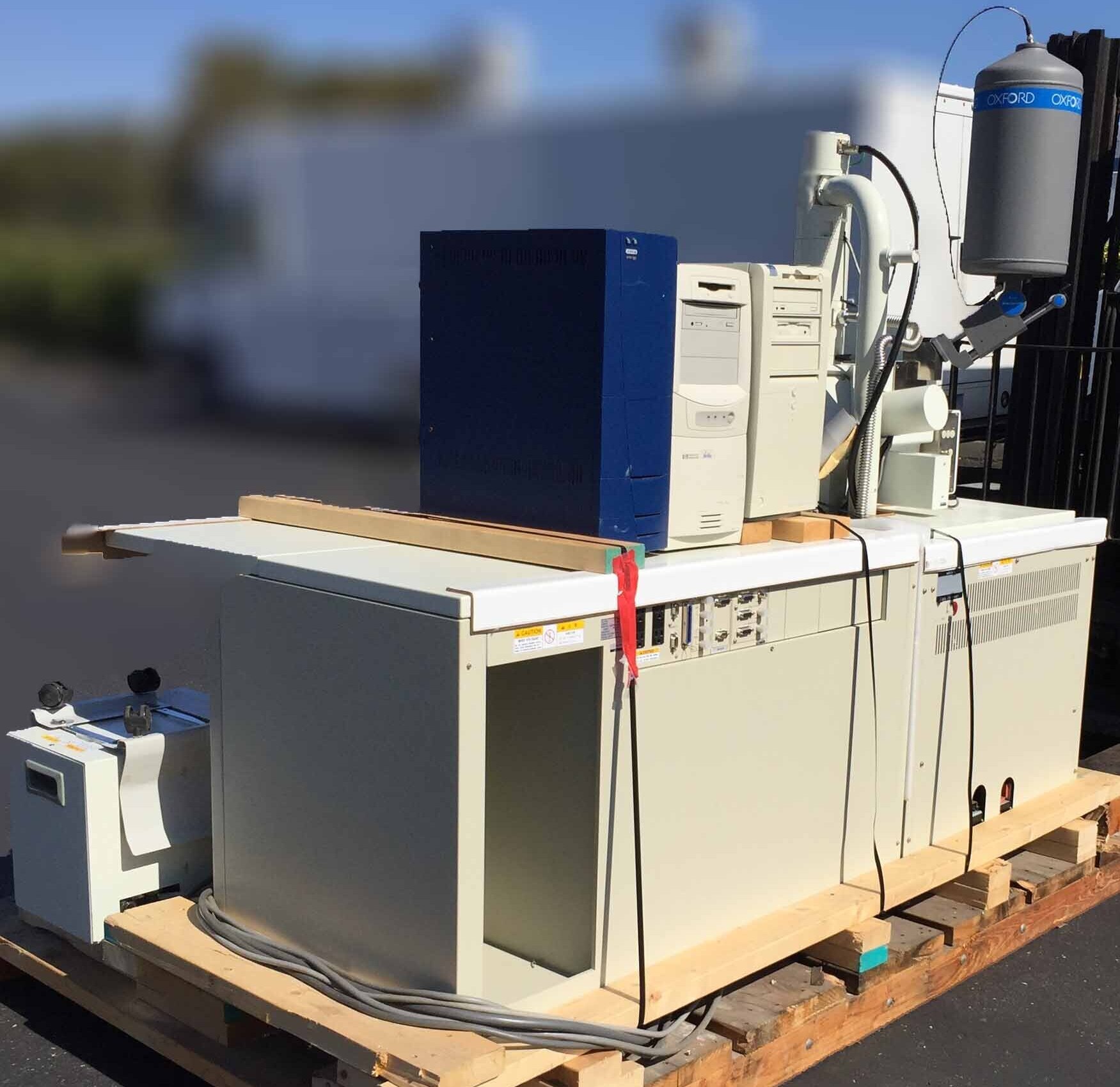
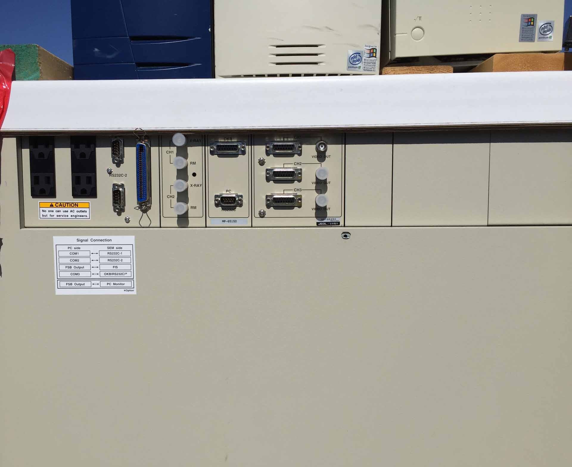
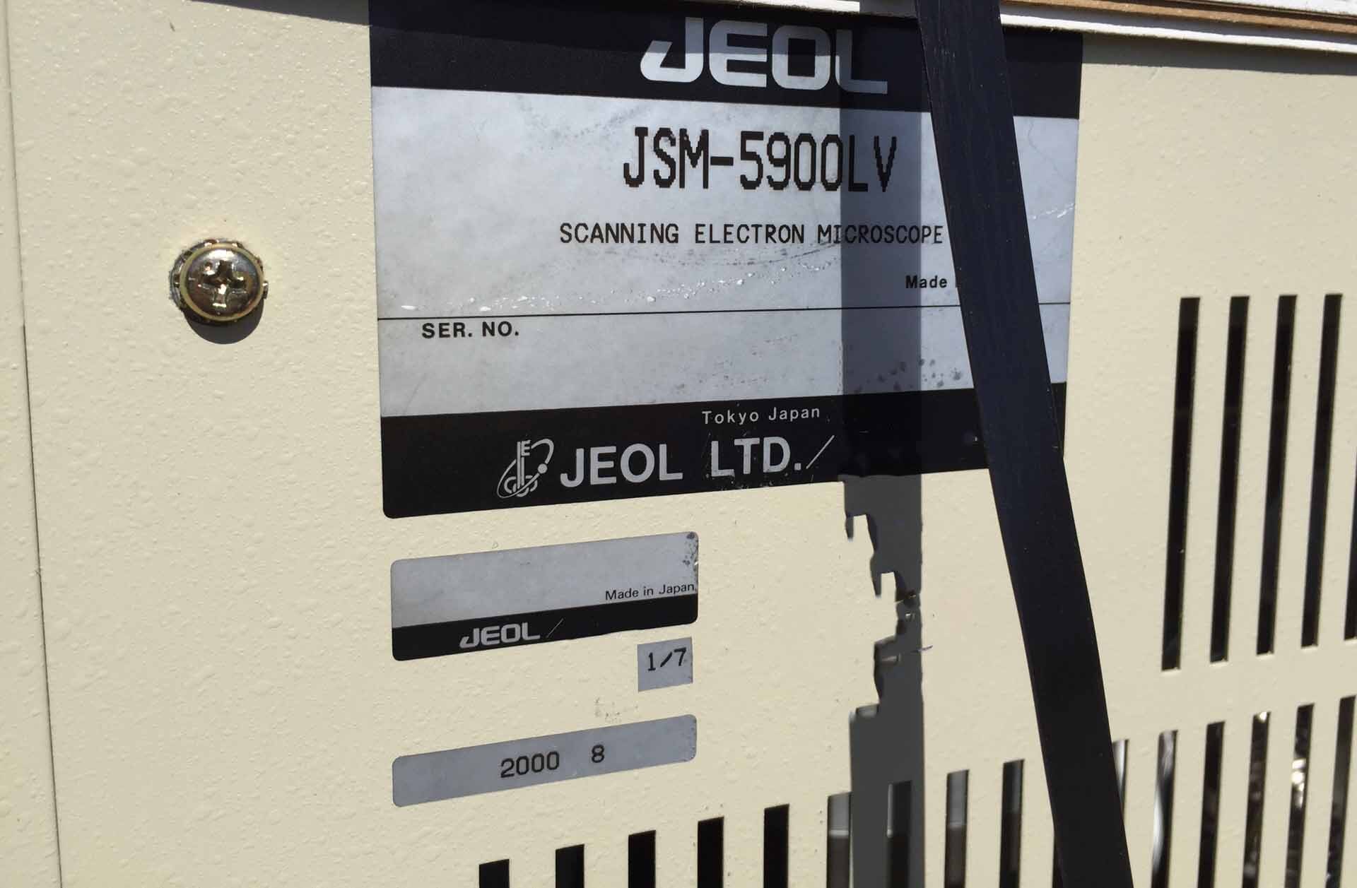
ID: 293743791
Vintage: 2000
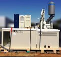
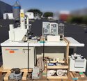
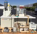
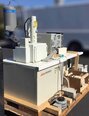
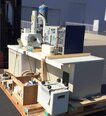
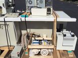
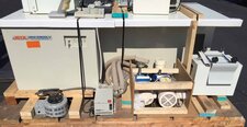
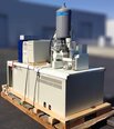
Scanning Electron Microscope (SEM)
OXFORD X-Ray detector
ULVAC Pumps
Transformer
Manuals
Cables
PC
2000 vintage.
JEOL JSM 5900LV scanning electron microscope (SEM) is an all-purpose imaging tool for high-resolution and 3D imaging and analytical applications. It is especially well-suited for nanoscale semiconductors, characterizing defects/features, and analyzing thin films. The device is known for being user-friendly and easy to operate, even for less experienced operators, while also providing excellent performance. JEOL JSM-5900LV features a variable pressure environment, enabling the user to apply a range of pressures for various types of applications. This adjustable pressure environment enables the microscope to operate in ultra-high vacuum (UHV) mode or low vacuum (LV) mode. UHV mode is best used for semiconductors and other applications requiring high magnifications. LV mode can be used for observing non-conductive specimens, such as biological samples and organic materials. The main imaging technique offered by the SEM is secondary electron (SE) imaging, which is used to create topographical images for morphology observations. With the SEM's high resolution SE detector, it can achieve up to a resolution of 500x106 pixels/µm2. It is also capable of reconstructing 3D images with "waffle images", which allow for sample imaging in a shorter acquisition time than backscattered (BSE) imaging. JSM 5900 LV is also highly versatile for semi-quantitative X-ray microanalysis with its large-area X-ray detector, which can be used to measure a wide range of element concentrations or peak energies. The SEM also facilitates an automated integrated mapping with its Advantage S software, which allows the user to generate compositional or element maps in a few minutes. In addition, JSM-5900LV provides simultaneous imaging and characterization with various detectors. With its Everhart-Thornley (ET) detector, the microscope can capture images of backscattered electrons (BSE), Auger electrons, and secondary X-ray (SXe) simultaneously. This feature makes the SEM beneficial for various materials, such as conducting, semi-conducting, and insulating specimens. To conclude, JEOL JSM 5900 LV scanning electron microscope is an excellent choice for a variety of imaging and characterization applications. It is a versatile, user-friendly device that offers high resolution imaging, 3D- reconstruction capability, and automated X-ray mapping. Its various detectors as well as its adjustable pressure settings give the user the ability to analyze a wide range of materials, from semiconductors to biological samples.
There are no reviews yet