Used JEOL JSM 5900LV #9230474 for sale
URL successfully copied!
Tap to zoom


ID: 9230474
Vintage: 1999
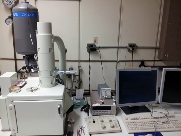
Scanning Electron Microscope (SEM)
EDX System
LINK ISIS Spectrometer 0738
7274 Detector
ATW2, 133ev, 10mm
Computer
Below the lens BSE detector
Requires LN
Cannot be converted to SDD type that does not use LN
Diffusion pump
Tungsten based system: 1 to 25 kV operating range
Objective aperture strip: 3, 20, 30, 100 um
Take off angle value: TA 35
Image detector ports: (2) Vacant ports plus the EDX
Maximum SEM resolution: 2560 x 1920
EDX resolution: 133 ev, ~1024 Pixel image resolution
No film camera
Circular port diameter: 120 mm
Optical resolution: 3.5 nm
Calibration of the gun bias is electronic
(2) PC's
(2) LCD's
(2) RP's
Transformer 100 V
Spectrometer box (same size as a PC)
Manuals
No printer
Ranges:
WD 5-40 (Limited by the under the lens BSE detector)
X and Y: Currently using 4" x 5" holder
Tilt: 90, Z: 48, X: -75 to 50mm, Y: -50 to 50 mm
1999 vintage.
JEOL JSM 5900LV is a scanning electron microscope (SEM) that is designed to offer high-level imaging capabilities with optimal resolution and speed. It features an ultrafast, large-stage sample holder with a magnification range of 5x to 50000x, allowing for a broad range of industrial, biological and geological research applications. The instrument is equipped with the latest electron optical technologies, with an amazing level of stability and accuracy. Its reflectance detectors and digital imaging allow for a detailed visualization of ultrafine structures and nanostructures with a resolution of down to 1nm. This microscope is enabled with a multiple-field scanning system that enables the user to capture several images at a time while keeping the same image quality. Furthermore, JEOL JSM-5900LV SEM also features a low-vacuum environmental chamber, which preserves the surface of delicate samples during the imaging process. The instrument is lightweight and compact and provides the same performance as larger models. It has a user-friendly control system, which allows the operator to navigate and adjust semiconductor imaging parameters without difficulty. This includes adjusting the angle of the electron beam, illuminating the sample at different angles, and adjusting deflection and acceleration voltages. JSM 5900 LV SEM is also compatible with a wide array of detectors and stage accessories. This includes a backscattered electron detector, an energy dispersive X-ray detector, a reflected electron detector, a surface probe detector, and an adjustable specimen holder. These accessories can be swapped out quickly to increase analysis capabilities. JSM 5900LV is a powerful and reliable scanning electron microscope offering superior image quality and atomic-level resolution. Its advanced electron optics and low-vacuum chamber make it perfect for a variety of research applications and it is suitable for a wide range of users. With an ergonomic design, user-friendly interface, and customizable accessories, the SEM is ideal for researchers in the biomedical, materials science, nanotechnology, and other scientific fields.
There are no reviews yet


