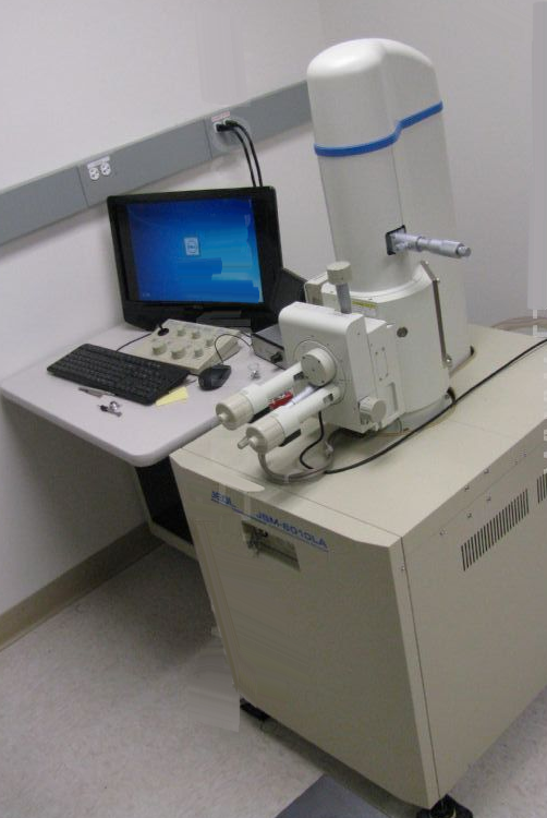
Used JEOL JSM 6010LA #9080849 for sale
It looks like this item has already been sold. Check similar products below or contact us and our experienced team will find it for you.
Tap to zoom


Sold
ID: 9080849
Scanning electron microscope (SEM)
Equipped with:
Energy Dispersive Spectroscopy (EDS)
Silicon Drift Detector (SDD)
onboard turbo pump
Resolution High Vacuum mode: 4nm (20kV), 8nm (3kV), 15nm (1kV)
Low Vacuum mode: 5nm (20kV) BSE
Accelerating voltage 500V to 20kV
Magnification x5 to x300,000 (printed as a 128mm x 96mm micrograph)
LV detector Multi-segment BSED (std.)
LV-SED (option)
LV pressure 10 to 100 Pa
Maximum specimen size Observation£º125mm diameter
Loadable 152mm
LGS type stage Eucentric goniometer
X=80mm, Y=40mm, Z=5mm-48mm
R=360¡ã (endless)
Tilt -10/+90¡ã
(Computer-controlled 2 or 3-axis motor drive)
Frame Store Up to 5120¡Á3840 pixels
EDS Standard (LA Version)
Embedded EDS system (silicon drift detector technology) Includes: Spectral Mapping, Multi-Point Analysis, Automatic Drift Compensation
Joel JSM-6010LA Microscopes Main Controls
Table Top
Table Base/Power Box
Monitor
Computer
Cords and Cables
Misc Accessories and Parts
Voltage: 100 V
Frequency: 50/60 HERTZ
InTouchScope function:
High resolution imaging in HV/LV/SE/BSE
Chemical analysis with integrated EDS built (standard on LA model)
Multi-touch screen control and wireless operation
Automatic SEM condition setup based on sample type
Simultaneous multiple live image and movie capture
Fast sample navigation at 5x ¨C 300,000x magnifications.
JEOL JSM 6010LA is a scanning electron microscope (SEM) designed for a wide range of imaging and analytical applications. The scanning electron microscope enables users to form two-dimensional images of the external surfaces of their sample. It is often used for detailed surface and topographical studies. This model utilizes a unique double beam technology, which combines an accelerated electron gun and a monochromated detector to enable both routine micro analysis and semiconductor failure analysis. The high resolution and high throughput of the instrument make it ideal for analyzing a wide range of nanoscale materials and objects. The high-performance scanning electron micrography of JSM 6010LA provides excellent imaging capabilities. The instrument has a resolution of 1 nm for secondary electrons and 0.25 nm for backscattered electrons. The analytical capabilities of JEOL JSM 6010LA are comprehensive. The instrument features an energy-dispersive X-ray spectrometer for elemental analysis of samples and a field emission gun for depth profiling. The spectroscopic feature can be used to measure X-ray line energy with an accuracy of 0.5 eV. The energy-dispersive X-ray spectral quantification offers preparation-free trace element analysis to the ppm level without any sample preparation. JSM 6010LA also has an in situ nanomechanical testing tool, enabling studies of the properties of sample surfaces from elastic to plastic mechanical deformation. This tool is used for analyzing the fracture surfaces of materials subjected to fracture testing. To facilitate ease of operation and automation, JEOL JSM 6010LA has several advanced features. It is equipped with an automated stage control system and a motorized SEM column with an automated, self-locking system for maintaining specimen position. It also possesses a liquid nitrogen condenser that allows sample holders of variable heights to be handled. Overall, JSM 6010LA is an accurate, reliable, and efficient scanning electron microscope designed for advanced imaging and analysis. Its excellent imaging and high-resolution capabilities make it an excellent tool for a wide range of studies.
There are no reviews yet