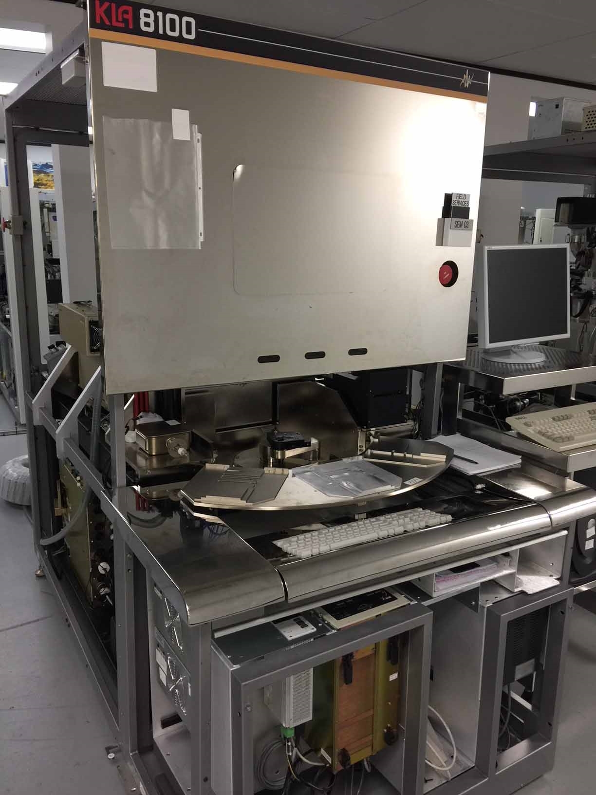
Used KLA / TENCOR 8100 #9203296 for sale
It looks like this item has already been sold. Check similar products below or contact us and our experienced team will find it for you.
Tap to zoom


Sold
KLA / TENCOR 8100 is a scanning electron microscope (SEM) with high performance, designed for both imaging and compositional analysis. It features a cold field emitter source and a high performance SE detector. The electron optical system is based on an advanced column design, providing exceptional imaging capability over a wide range of working distances and magnifications. The microscope is capable of sub-nanometer resolution imaging and, in the low-emission mode, can accommodate small beam sizes for compositional analysis. KLA 8100 has a high analytical sensitivity and offers advanced scan and precision control for efficient imaging and compositional analysis. It is capable of depth profiling to analyze the chemical composition in the depth direction. It has a built-in optically enhanced backscatter detector and dual ion detectors that measure the ion energy spectrum for elemental mapping and compositional analysis. TENCOR 8100 offers a wide range of automation capabilities for user-friendly workflows, including specimen handling, sample orientation detection, automated image capture, and integrated tasks like image stitching. The microscope can be used in combination with low and medium vacuum measurement stages for alignment and handling automatic SEM sample exchange between the microscope and vacuum stages. 8100 produces images with excellent contrast and high signal to noise ratio at low beam currents, thus allowing the user to obtain maximum detail and large field of view with minimum charging artifacts. The automated functions and software-controlled image synthesis reduce the operator time for multivariate analysis. KLA / TENCOR 8100 is an ideal tool for semiconductor failure analysis, studying a wide range of materials such as metals, ceramics, inorganics, composites, industrial polymers, and biological samples. It is also suitable for the characterization of device structures, assessing surface morphology and lithographic defects, and measuring particle size, shape, and surface roughness.
There are no reviews yet