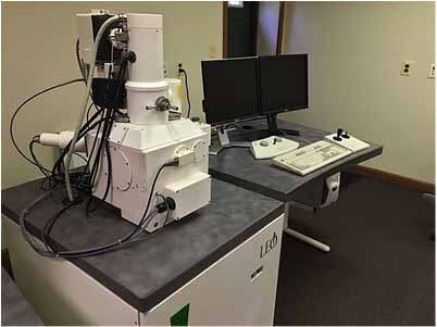
Used LEO / ZEISS 1450 #9161452 for sale
URL successfully copied!
Tap to zoom


ID: 9161452
Scanning electron microscope (SEM)
Electron source: Tungsten
Resolution:
2.5nm at 30kV (LaB6)
3.5nm @30kV (W)
5.5nm @30kV (BSD-VP mode)
Includes:
EDS
EBSD
Magnification range: 9x to 900000x
Probe current
1pA to 1uA Optibeam controlled
Accelerating voltage: 200 V to 30kV
Variable pressure: 1Pa to 400Pa
Detectors: Everhart thornley with VPSE / VPSE or BSD
Chamber: 300 mm x 270 mm x 224 mm (H)
5-Axis motorized stage:
X-Travel: 100 mm
Y-Travel: 125 mm
Z-Travel: 60 mm (35 mm motorized)
Rotation: 360° continuous
Tilt: 0° to 90°
Image processor resolution: Up to 3072 x 2304
Image processing:
Pixel averaging
Continuous averaging
Frame integration
Oil diffusion pump main vacuum
Roughing pump
~1999 vintage.
LEO / ZEISS 1450 scanning electron microscope (SEM) is a high resolution imaging tool that uses electrons to create detailed images of samples of various sizes and materials. LEO 1450 SEM operates by generating a focused beam of electrons which is scanned over the sample using a deflecting system. By controlling the angle of incidence of the beam, it is possible to generate a three-dimensional image of the sample. As the electrons are specific to each element, it is possible to create elemental maps which show the concentrations of each element in the sample. ZEISS 1450 SEM is equipped with two electron sources which operate with energies of up to 10kV and 30kV respectively. This allows a wide range of materials to be imaged including insulators and conducting materials. The resolution of the images generated by the machine is also very high reaching a lateral resolution of up to 0.5nm and an axial resolution of up to 0.25nm. Furthermore, 1450 SEM is equipped with a variety of detectors which enable it to receive signals from the specimen. These include a Faraday cup which is used to measure the beam current, a scintillation counter used to detect low-level energy X-rays from the sample, an energy dispersive spectroscopy (EDS) detector used to map the elemental composition of the sample, and a back-scattered electron (BSE) detector used for imaging the surface topography of the sample. LEO / ZEISS 1450 SEM is also capable of quantitative analysis which involves measurement of parameters such as grain size, volume, porosity, thickness of films, surface area and surface texture. It is also able to perform spectroscopic analysis, making it possible to measure a variety of properties such as composition, optical constants, impedance, dielectric constants and magnetism. In conclusion, LEO 1450 SEM is a powerful tool which is used for the analysis and imaging of samples with a wide range of materials and sizes. It provides high-resolution images, quantitative analysis and spectroscopic analysis, making it an invaluable tool for research and industrial applications.
There are no reviews yet