Used LEO / ZEISS 1455 #9162511 for sale
URL successfully copied!
Tap to zoom









ID: 9162511
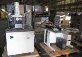
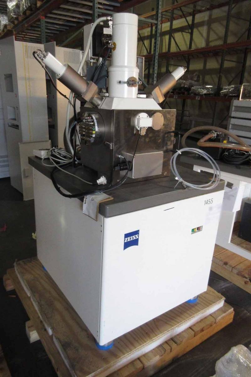
Scanning electron microscope (SEM)
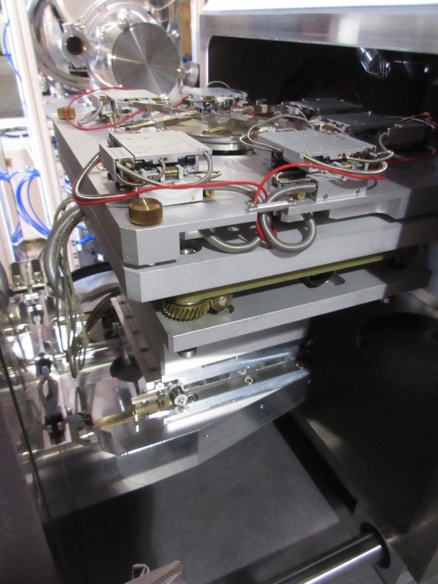
Nano prober
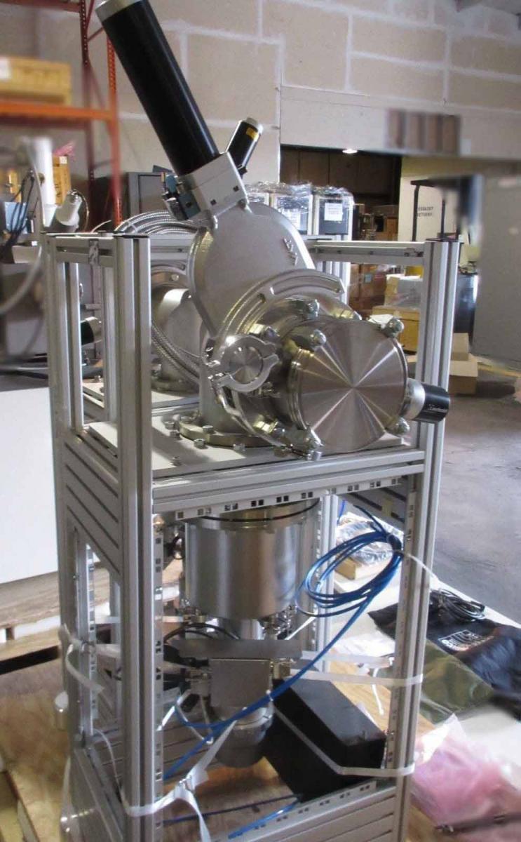
Cryogenic assembly
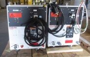
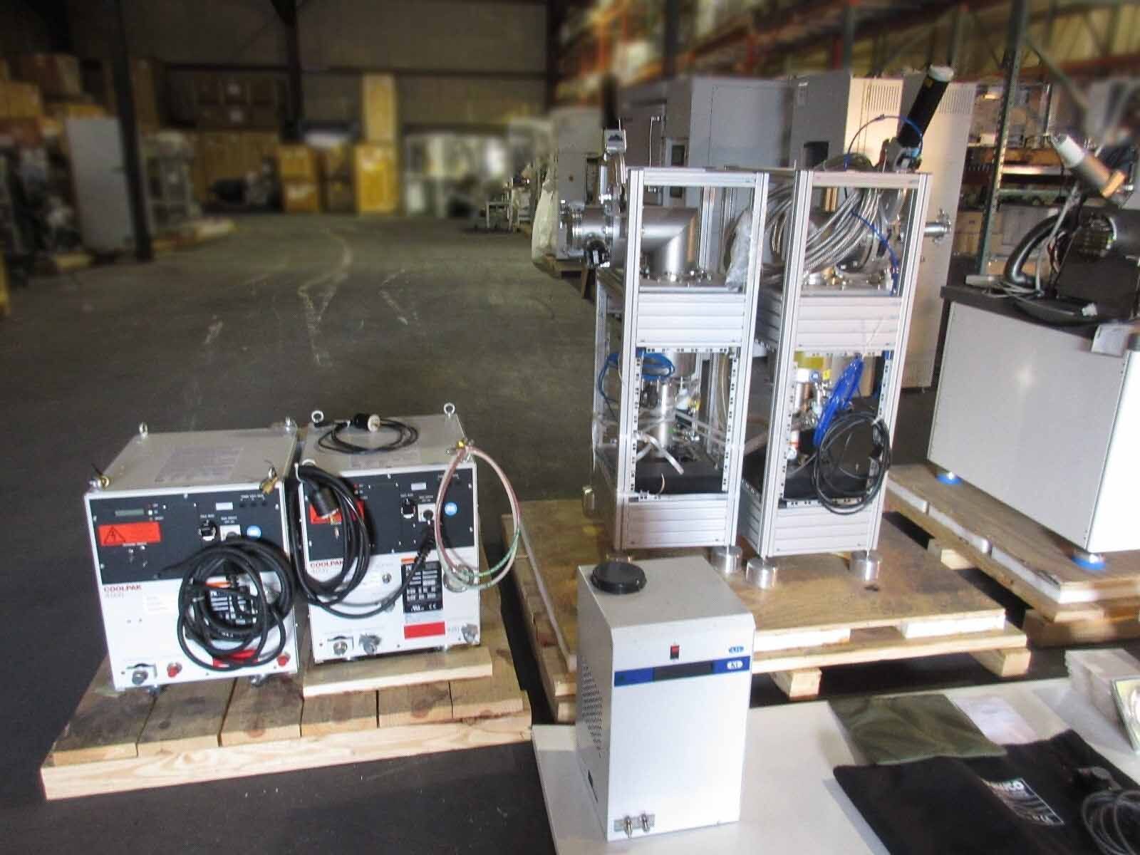
(2) LEYBOLD coolpak 4000 cryo compressors
Model no: Coolpak 4000
(2) VAT Gate valves, model no: 12144-PA44-0001
(2) OERLIKON LEYBOLD sensors, model no: 230070
(2) LEYBOLD 3000 CL coolvac cryo compressors
Main body
(1) KAMMRATH & WEISS ZR stage controller
(1) Zyvex IC nanoprober system
Four needle prober module
(1) HITEK Power supply, Model no: G303 / 56
(1) Varian TV 301NAV turbo pump controller, model no: 9698918S011
(1) HITEK power supply, model no: 1P100 / 502 / 05 A1021120
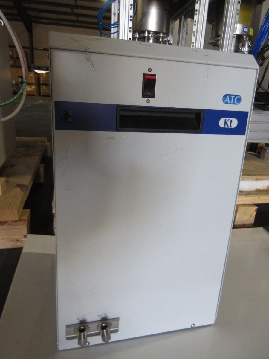
Chiller
ATC Applied thermal control chiller, model no: KTR6000
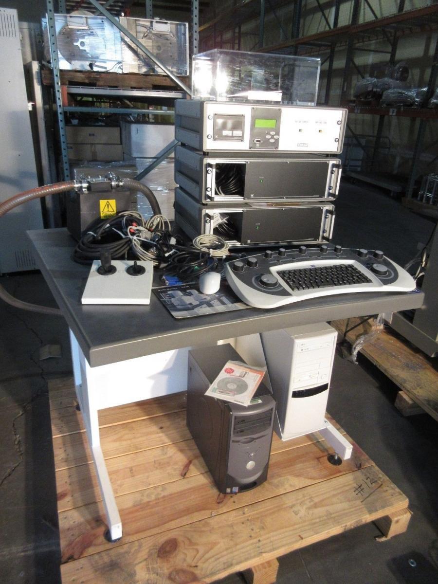
Controllers
(1) LEYBOLD center one
(1) LEYBOLD coolvac SC
(2) LEYBOLD coolvac PS
(1) Dell Pentium 4 desktop computer
(1) Desktop computer, model no: 3475239010200
(1) KAMMRATH and WEISS micro module controller
(1) KAMMRATH and WEISS joystick prober controller
(1) Prober stage piezo and motor controller
(1) KEITHLEY 708A switching system
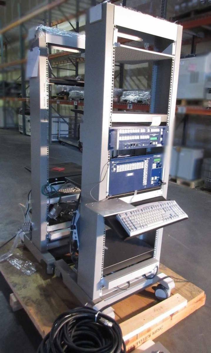
(1) Analog way graphic switcher 2
(16) Computers and video inputs
Seamless switcher
Mixer / Scaled data output, model no: GSW2814
(1) Analog way 1x graphic switcher remote controller unit, model no: RCU 2811A
Miscellaneous
(1) COHU CCD camera, model no: 22521040 / 0000.
LEO / ZEISS 1455 is a Scanning Electron Microscope (SEM) designed for use in a variety of laboratory and research settings. This device is an invaluable tool for scientists in the study of materials on a nanometer scale and for the rapid analysis of advanced materials. The main components of LEO 1455 include an electron source, a detection system, an x-y stage, and an electron gun. The electron source emits a low-energy, high-current beam of electrons, which pass through the sample and reach a detection system. The detection system then records the interactions between the electrons and the sample. The x-y stage in ZEISS 1455 is a regulated translation stage, which provides step-by-step motion of the sample in two independent axes. This allows the user to precisely target the sample with the beam of electrons and precisely control the magnification of the image. The electron gun allows for a variety of beam sizes to be used for different configurations. 1455 produces high-resolution images of structures and surfaces on a nanometer scale. It offers both bright field and dark-field imaging, and the user can choose between multiple imaging modes such as secondary electron imaging, secondary neutral atom imaging, and backscatter electron imaging. The device is designed with an advanced electron optics which includes electrostatic and magnetic lenses to enhance image resolution. The energy resolution of LEO / ZEISS 1455 is extremely high, allowing it to achieve a resolution of up to 3nm in some configurations. The device is capable of producing images with as few as 6 electrons per pixel, and its electron detector can detect signals at low and high energies. The high signal-to-noise ratio of this device allows for the detection of even sub-10nm features. LEO 1455 features a range of automated parameters, from the positioning of the sample to the adjustment of imaging parameters. It is designed to be user-friendly, with a 7-inch touchscreen interface that allows the user to control the microscope quickly and easily. Overall, ZEISS 1455 is an excellent choice for scientists and researchers looking for a reliable and powerful SEM. It can provide high resolution images at extremely small scales, making it an invaluable tool for nanomaterials analysis and advanced materials research.
There are no reviews yet

