Used OMICRON / NANOTECHNOLOGY Microscope #293755064 for sale
URL successfully copied!


Tap to zoom
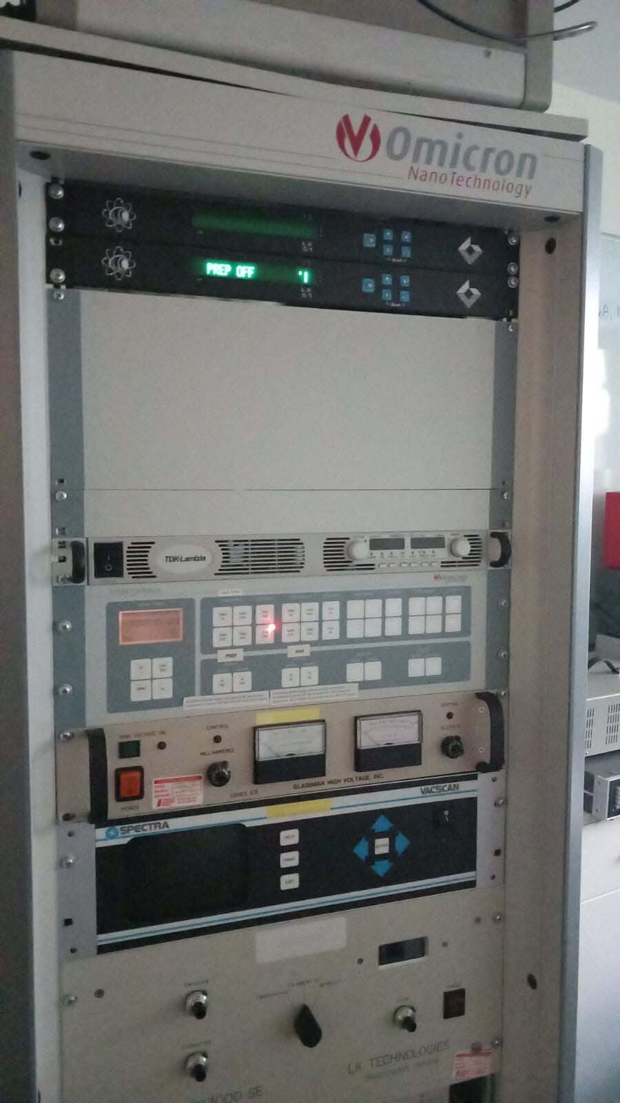

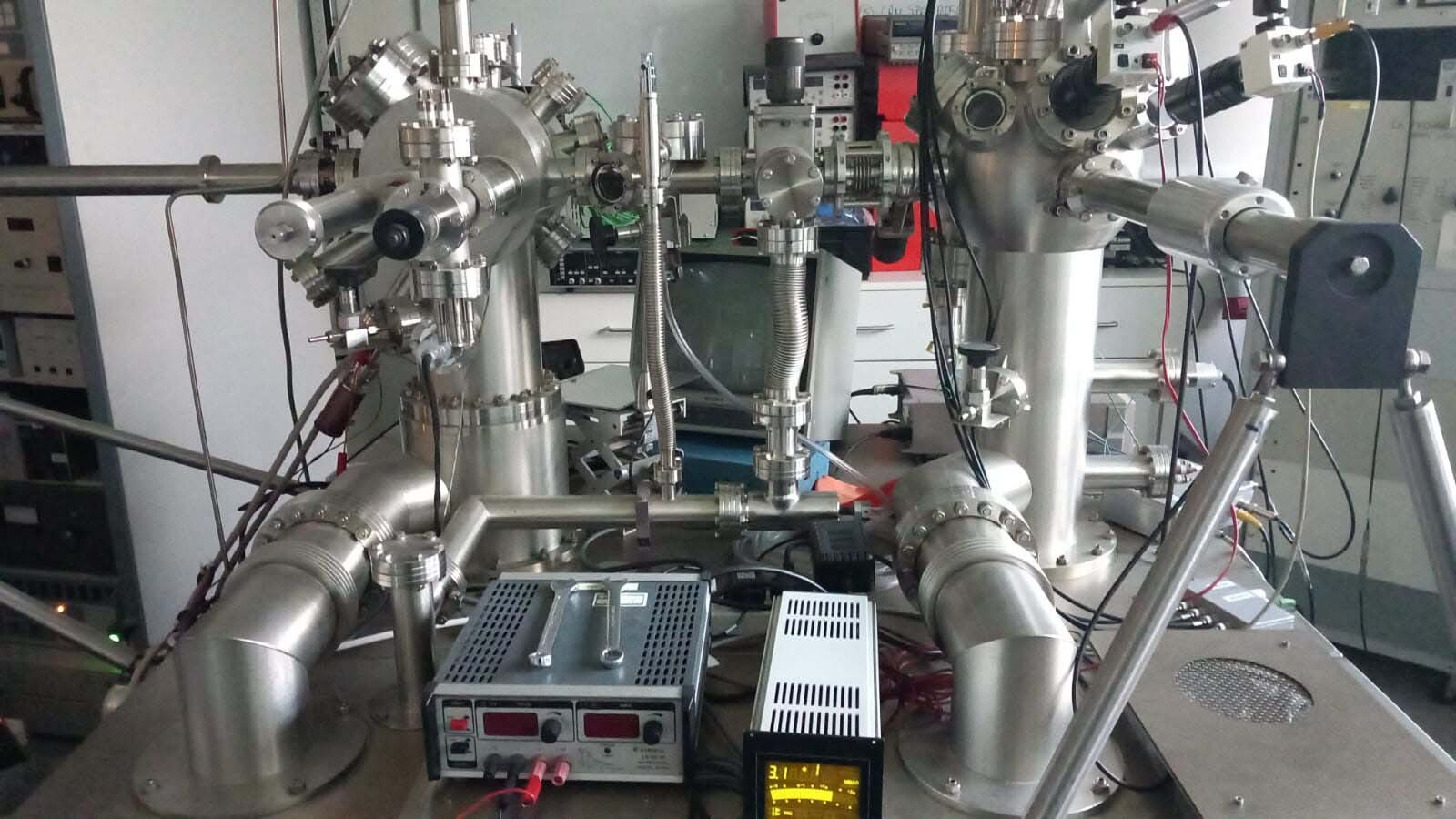
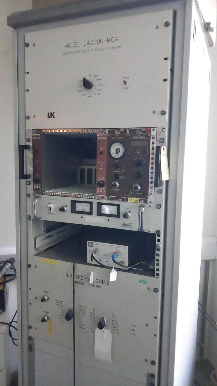
OMICRON / NANOTECHNOLOGY Microscope is a cutting-edge scanning electron OMICRON Microscope (SEM) that is designed for high-resolution imaging and detailed analysis at the nanoscale level. This powerful instrument incorporates state-of-the-art OMICRON features and capabilities to enable researchers and scientists to investigate a wide range of materials and structures with exceptional precision and accuracy. At the core of NANOTECHNOLOGY Microscope is its electron beam source, which generates a focused beam of electrons that is used to scan the surface of the sample under investigation. The high-energy electrons interact with the atoms in the sample, producing signals such as secondary electrons, backscattered electrons, and characteristic X-rays. These signals are detected and analyzed to create highly detailed images and gather valuable information about the sample's composition, morphology, and topography. One of the key features of Microscope is its high-resolution imaging capability, which allows users to observe and analyze samples with exceptional clarity and detail. The instrument is equipped with advanced detectors and imaging systems that can capture images with sub-nanometer resolution, revealing tiny surface features and structures that are not visible with conventional microscopes. In addition to imaging, OMICRON / NANOTECHNOLOGY Microscope offers a range of analytical techniques that enable researchers to perform in-depth investigations of the samples. For example, energy-dispersive X-ray spectroscopy (EDS) can be used to analyze the elemental composition of the sample by detecting characteristic X-rays emitted during electron interactions. This technique provides valuable insights into the chemical composition and distribution of elements within the sample. Another powerful analytical tool available on OMICRON Microscope is electron backscatter diffraction (EBSD), which can be used to analyze the crystallographic orientation and grain structure of materials. By measuring the patterns of backscattered electrons, researchers can determine the crystallographic phases present in the sample and study grain boundaries, defects, and texture. NANOTECHNOLOGY Microscope also offers advanced imaging modes, such as field emission SEM (FE-SEM) and environmental SEM (E-SEM), which allow users to study samples under various conditions. FE-SEM provides increased resolution and sensitivity compared to conventional SEM, making it ideal for imaging delicate samples and low-conductivity materials. E-SEM enables imaging of samples in a controlled environment, such as low vacuum or wet conditions, to study dynamic processes and interactions. Furthermore, Microscope is equipped with sophisticated software for data acquisition, processing, and analysis. Users can perform image processing, elemental mapping, 3D reconstruction, and quantitative analysis to extract valuable information from the acquired data. The intuitive user interface and automation capabilities streamline workflow and enable efficient operation of the instrument. Overall, OMICRON / NANOTECHNOLOGY Microscope is a state-of-the-art SEM system that combines NANOTECHNOLOGY innovations with high-performance imaging and analytical capabilities. With its advanced features, exceptional resolution, and versatile applications, this instrument is a valuable tool for researchers in materials science, OMICRON / NANOTECHNOLOGY, biology, geoscience, and other fields seeking to explore the nanoworld with precision and detail.
There are no reviews yet