Used ZEISS Scanning Electron Microscope (SEM) #293763916 for sale
URL successfully copied!
Tap to zoom
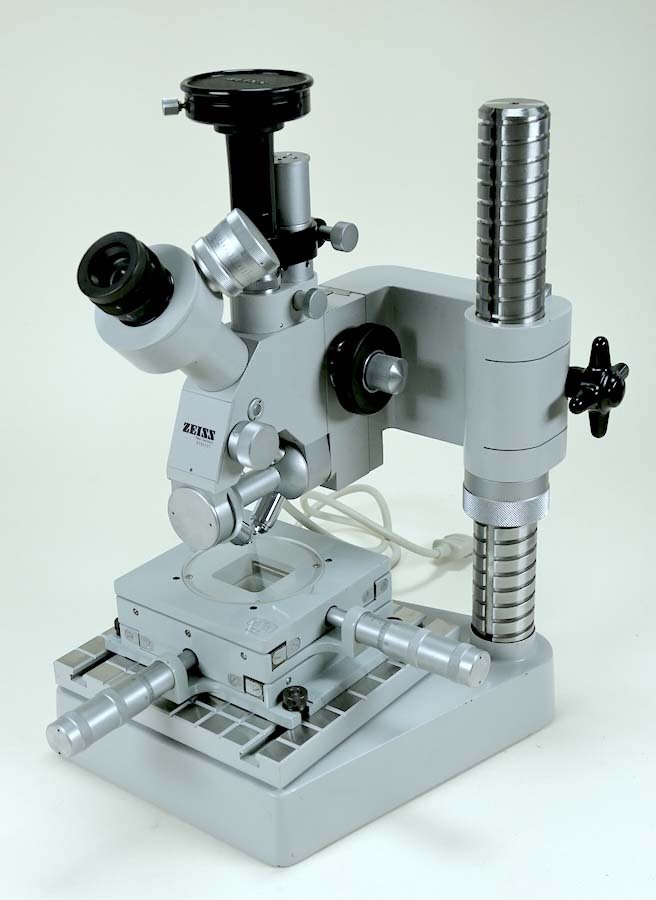

ID: 293763916
A ZEISS (Carl ZEISS AG) Scanning Electron Microscope (SEM) is an advanced analytical instrument that utilizes electron microscopy techniques to investigate the surface topography and composition of specimens at a nanometer scale. SEMs are essential tools in various fields such as materials science, nanotechnology, biology, and geology for their ability to provide high-resolution imaging and elemental analysis. The key components of a ZEISS SEM include an electron source, electron lenses, specimen chamber, detectors, and a high-resolution imaging system. The SEM operates by generating a focused beam of electrons that is scanned across the specimen surface. The interaction between the electrons and the specimen generates various signals that are used to form detailed images and acquire valuable data. The electron source in a ZEISS SEM typically consists of a tungsten filament that emits electrons when heated. These electrons are accelerated towards the specimen by a series of electromagnetic lenses, which focus the beam to a sub-nanometer spot size. The high energy of the electrons allows for deep penetration into the specimen, enabling imaging of internal structures and providing detailed information about the sample composition. The specimen chamber of the SEM is designed to hold samples in a controlled vacuum environment to prevent electron scattering and ensure optimal imaging conditions. Various specimen holders and stages are available to accommodate different sample sizes, shapes, and types. The detectors in the SEM detect the signals generated by the interacting electrons and the specimen, such as secondary electrons (SE), backscattered electrons (BSE), X-rays, and cathodoluminescence. Secondary electron imaging is a widely used technique in SEM that provides high-resolution topographical information about the sample surface. Secondary electrons are emitted from the specimen's surface due to the impact of the incident electron beam, creating detailed images with high depth of field. Backscattered electron imaging, on the other hand, provides contrast based on variations in sample composition, density, and atomic number. In addition to imaging, a ZEISS SEM is equipped with energy-dispersive X-ray spectroscopy (EDS) capabilities for elemental analysis. EDS detectors capture characteristic X-rays emitted by the specimen when bombarded by the electron beam, enabling the identification of elements present in the sample and their distribution. This feature is essential for mapping elemental compositions, identifying phases, and analyzing chemical compounds in a wide range of materials. ZEISS SEMs are known for their high-resolution imaging capabilities, with spatial resolution reaching sub-nanometer levels, depending on the operating conditions and sample characteristics. The advanced imaging systems, coupled with sophisticated software for image processing and analysis, allow researchers to visualize and investigate structures at the atomic scale, providing valuable insights into the properties and behavior of materials. Overall, a ZEISS Scanning Electron Microscope is a powerful tool for characterizing and analyzing a wide range of samples with high precision and detail. Its versatility, high-resolution imaging, and elemental analysis capabilities make it an essential instrument for scientific research, quality control, and technological advancements across various disciplines.
There are no reviews yet