Used ZEISS Scanning Electron Microscope (SEM) #293765879 for sale
URL successfully copied!




Tap to zoom
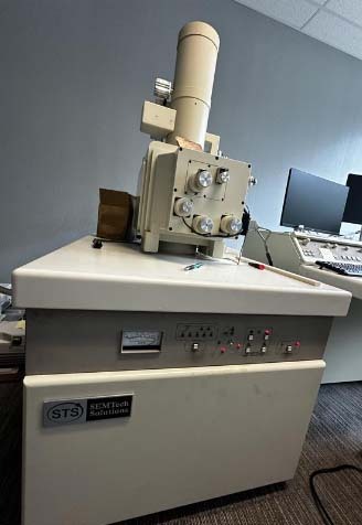

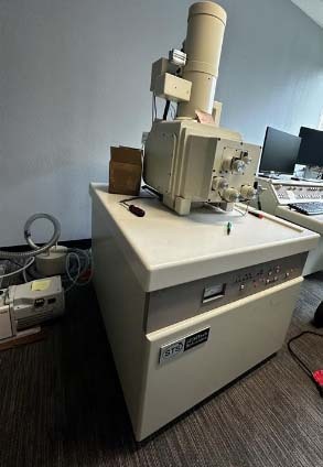
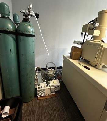
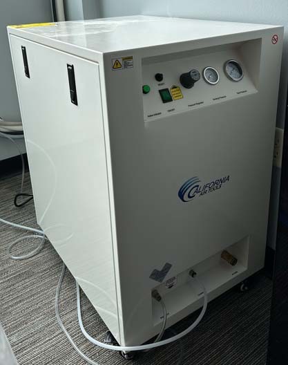

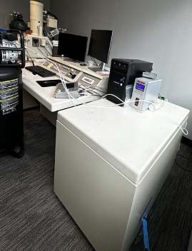
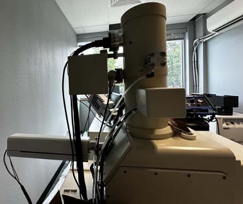
ID: 293765879
ZEISS Scanning Electron Microscope (SEM) is a powerful imaging instrument that utilizes an electron beam to produce high-resolution images of sample surfaces. SEMs are widely used in various scientific and industrial applications to analyze the topography and composition of materials at the nanoscale level. ZEISS, a leading manufacturer of microscopy solutions, offers a range of SEM models with advanced features and capabilities that cater to diverse research needs. The basic working principle of an SEM involves generating a focused electron beam that scans across the surface of a sample. When the electrons interact with the sample, various signals are emitted, including secondary electrons, backscattered electrons, and characteristic X-rays. These signals are then detected and processed to create detailed images that reveal the microstructure and chemical composition of the sample. ZEISS SEM is equipped with sophisticated electron optics that enable high-resolution imaging with exceptional clarity and contrast. The electron column typically consists of a thermionic electron source, electromagnetic lenses, and apertures that control the beam size and shape. ZEISS SEMs are designed to provide excellent resolution capabilities, allowing researchers to visualize features as small as a few nanometers in size. One of the key advantages of ZEISS SEM is its versatility in sample analysis. With the availability of different imaging modes and analytical techniques, users can obtain valuable information about the morphology, topography, and chemical composition of a wide range of materials. ZEISS SEMs are capable of producing 2D images, 3D surface reconstructions, elemental mapping, and line profile analysis, among other applications. In addition to imaging capabilities, ZEISS SEMs are equipped with advanced electron detectors that enhance signal detection and sensitivity. Detectors such as Everhart-Thornley detectors, in-lens detectors, and energy-dispersive X-ray spectroscopy (EDS) detectors allow for efficient imaging and elemental analysis of samples. The integration of EDS systems in ZEISS SEMs enables users to perform qualitative and quantitative chemical analysis with high accuracy. Moreover, ZEISS SEMs offer a range of imaging modes to suit different sample types and analytical requirements. These include secondary electron imaging for surface topography, backscattered electron imaging for compositional contrast, and variable pressure imaging for non-conductive samples. The flexibility in imaging modes allows users to adapt the SEM settings to optimize image quality and information retrieval. ZEISS SEMs are also equipped with user-friendly interfaces and software platforms that facilitate data acquisition, analysis, and visualization. The intuitive control software enables easy manipulation of imaging parameters, sample navigation, and image processing. Additionally, ZEISS offers advanced software packages for image analysis, particle counting, and automated measurements to streamline data interpretation and reporting. In summary, ZEISS Scanning Electron Microscope is a cutting-edge imaging tool that provides researchers and scientists with the capability to explore the microstructure and composition of materials at the nanoscale. With its high-resolution imaging, versatile analytical techniques, and user-friendly interface, ZEISS SEM is a valuable instrument for a wide range of applications in materials science, life sciences, geology, and nanotechnology.
There are no reviews yet