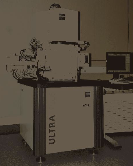
Used ZEISS Ultra Plus #9028799 for sale
It looks like this item has already been sold. Check similar products below or contact us and our experienced team will find it for you.
Tap to zoom


Sold
ID: 9028799
FE SEM
0.1 to 30 keV electron beam to image the surface of a sample in high vacuum
Edge resolutions down to 1 nanometer at 15 keV and 1.7 nm at 1 keV
Detectors available:
Inlens SE, Everhart-Thornley SE-BSE
EsB (inlens Energy selective Backscattered electron detector)
STEM (Scanning Transmission Electron detector)
80 mm airlock for sample exchange
Charge Compensation (CC) system:
Places a gas needle close to the sample for localized gas (N2) injection to reduce charging
CC system reduces the skirt effects observed in traditional variable pressure systems and the normal SE detectors (Inlens and Everhart-Thornley) can be used.
ZEISS Ultra Plus is an advanced scanning electron microscope (SEM) that can be used to observe the structure of materials at a very high resolution. This equipment features a high-performance electron column that allows for imaging to a resolution better than 5 nanometers. The electron column is coupled with a ZEISS field emission gun which provides low electron emission and excellent stability. This system also has micro-spot technology, ideal for imaging the structure of organic materials, and a high-resolution large area backscattered electron detector. Ultra Plus allows users to select the best operating conditions quickly and accurately, and is excellent for nano-structural application. In addition to high-resolution imaging capabilities, ZEISS Ultra Plus also offers option modules for electron beam lithography and in-situ heating, which can provide users with electric, chemical and thermal control for studies of hydrogen embrittlement, corrosion, oxidation and other material properties. Additionally, the device has an integrated spectroscopy module which can be used for energy-dispersive X-ray spectrometry and electron energy loss spectrometry. This spectroscopy module is especially useful for studying the composition of materials. Finally, Ultra Plus has a robust hardware and software platform, which includes automated alignment, drift correction, and advanced image processing techniques to help streamline workflows for maximum efficiency. Additionally, the device can be operated remotely, allowing for remote collaborations or remote access to data. ZEISS Ultra Plus also includes a sample loading unit, in-lens detector machine and sub-micron stitching capability. Together, these features allow users to easily prepare and observe materials with a variety of imaging techniques. In conclusion, Ultra Plus is an advanced scanning electron microscope that offers high-resolution imaging, in-situ heating and lithography, spectroscopy, automation and a unique hardware setup, making it ideal for nanostructural imaging and analysis. ZEISS Ultra Plus is an excellent choice for researchers and engineers looking for a robust and powerful SEM tool.
There are no reviews yet