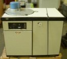
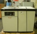
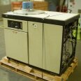
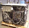
Used CVC 601 #9060536 for sale
URL successfully copied!
Tap to zoom





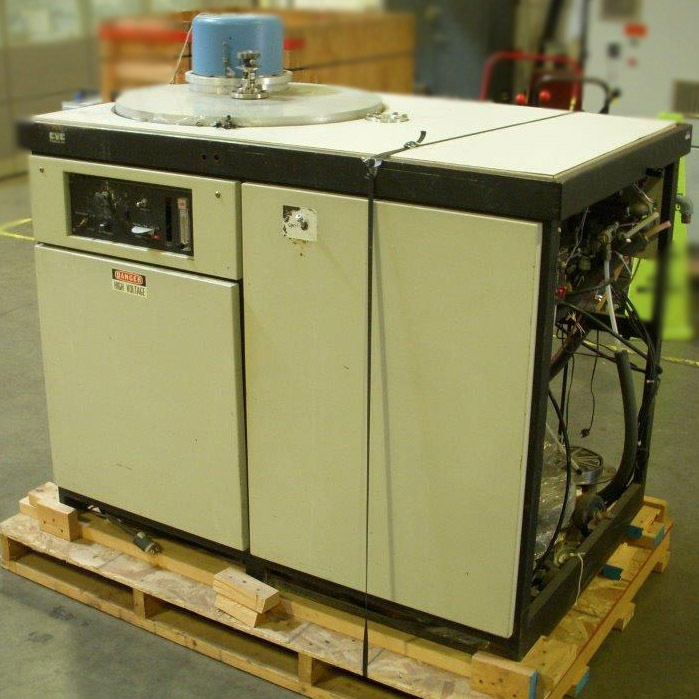

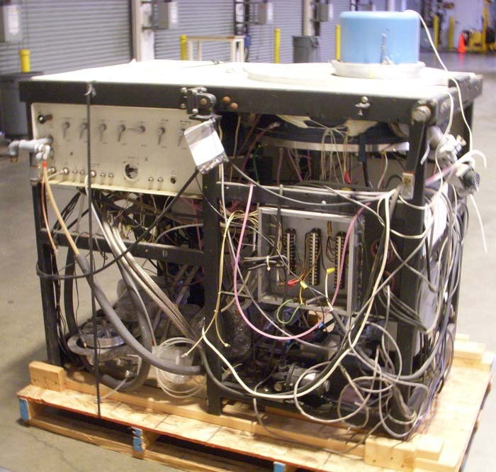

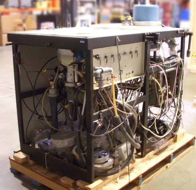

ID: 9060536
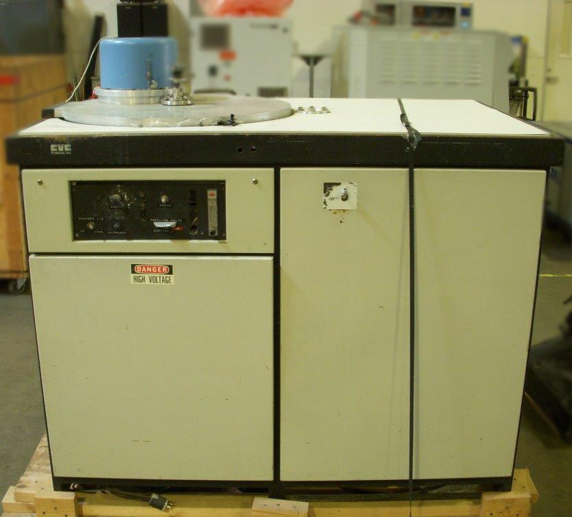
Sputtering system
Includes:
Cryo pump
Hivac valve
Air cylinder lift lid missing.
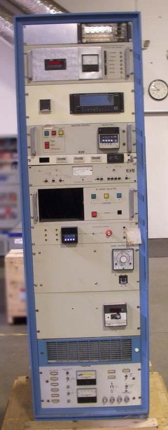
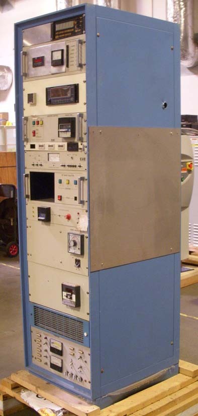
CVC 601 is a state-of-the-art direct current (DC) magnetron sputtering equipment. This system is designed for fundamental and applied research in microelectronics and optoelectronics device fabrication. It provides precise control over a variety of operating parameters to produce high quality thin films within a wide range of sputtering techniques. 601 has a modular design which allows a variety of configuration options to meet research and industrial needs. It is a true DC sputtering unit for oxidization, nitridation and other thin film applications. The 6" target machine utilizes advanced unbalanced magnetron sputtering sources which can be optimized to provide long life, high rate deposition and reproducible results. The high power RF tuning device is designed to ensure reliable and repeatable process control. CVC 601 includes a power supply section apparatus, heaters, shutter tool and a vacuum asset with turbo molecular pumps. The model is configured for controlling chamber pressure, base pressure and operating pressure, allowing for precise preparation of substrates to the required optimal pressure values. The precise control of operating temperatures is enabled by an advanced PID control equipment with high precision Pt1000 resistance thermometer. The software package for 601 system allows precise micron-level control of the target position, substrate position, and RF power supply settings. The onboard robotic arm enables automated substrate placement and retrieval for batch processing. Other features include an automated process control unit, an optical feedback cell, a process monitoring module, and a safety interlock machine for ensuring operator safety. Additionally, CVC 601 can be customized with an optional quick-disconnect gas distribution tool for evacuating and backfilling the chamber with different gases. 601 is an ideal tool for materials research, thin film deposition, and surface characterizations. It is suitable for various applications such as solar cells, flat panel displays, CMOS imaging devices, hard coatings, and MEMS devices. The combination of precise control over process parameters, a wide range of advanced features, and versatile software provides an outstanding user experience.
There are no reviews yet


