Used HITECH 300S / Tecmet 2000 #293714593 for sale
URL successfully copied!

Tap to zoom
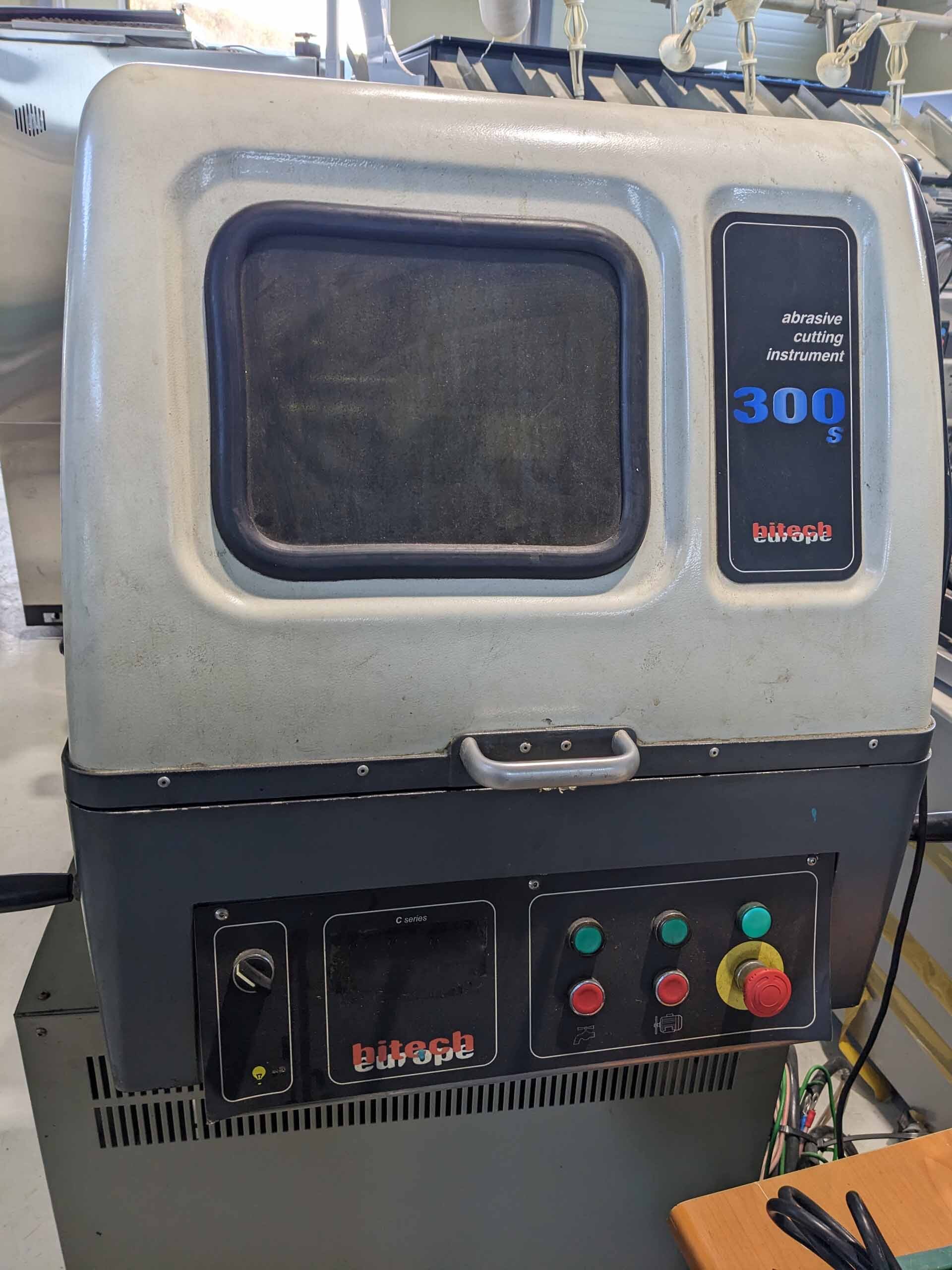

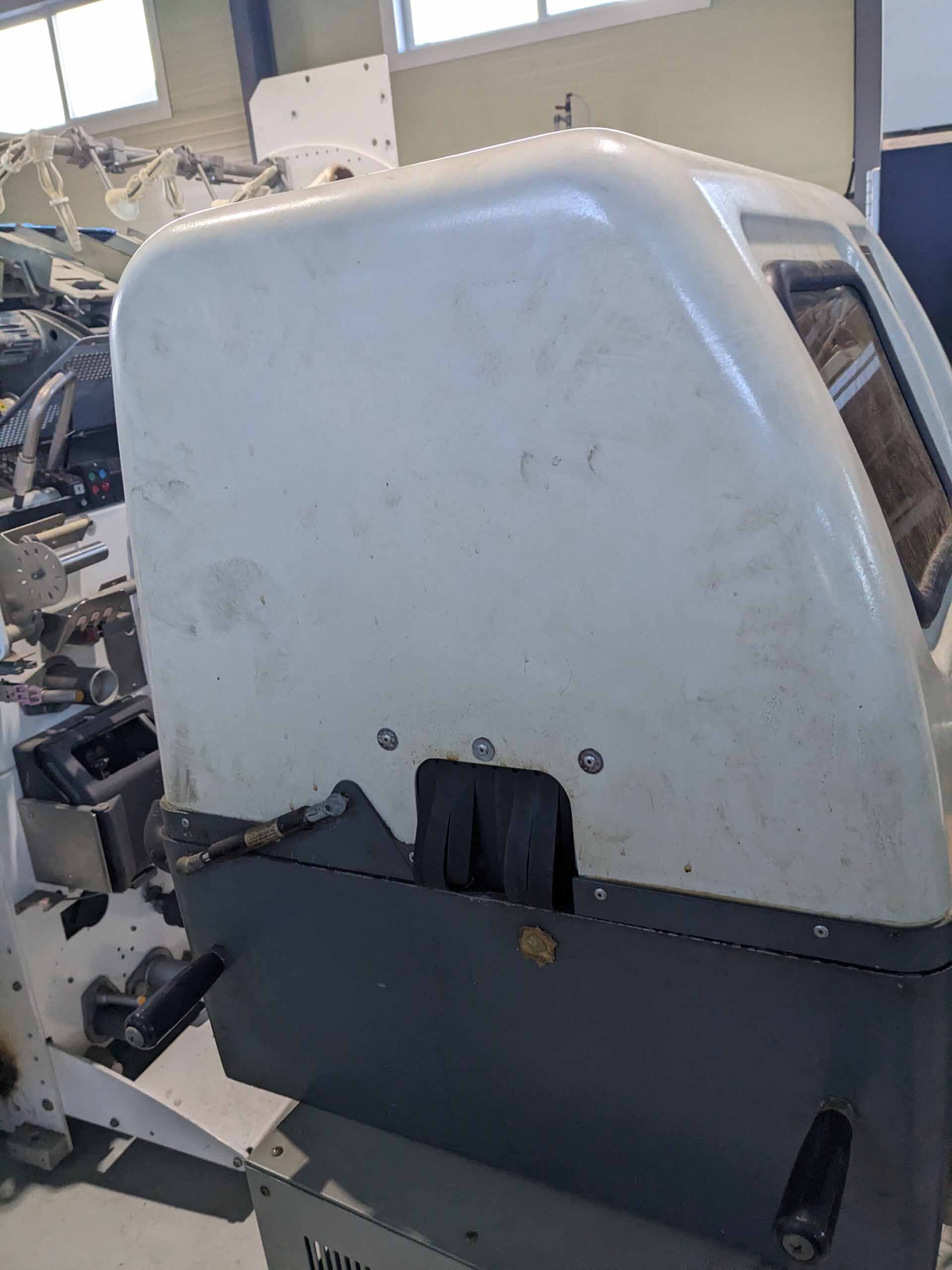
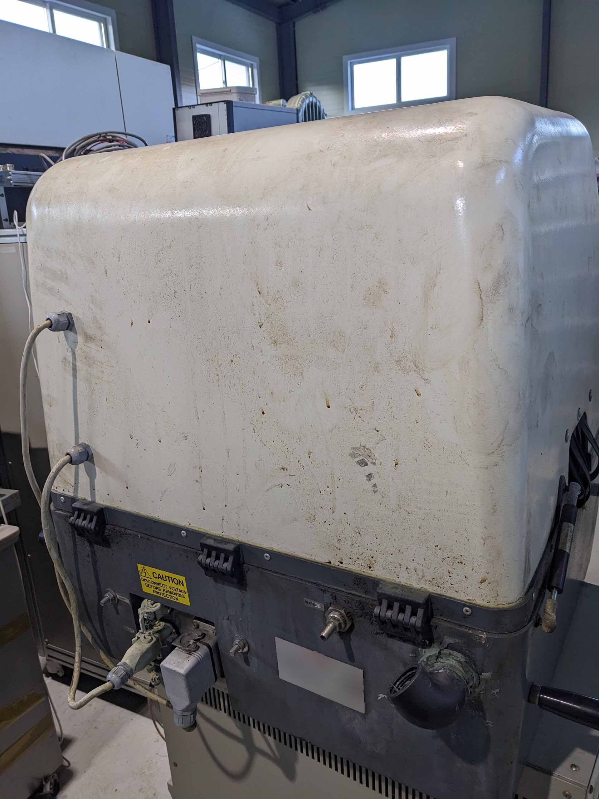
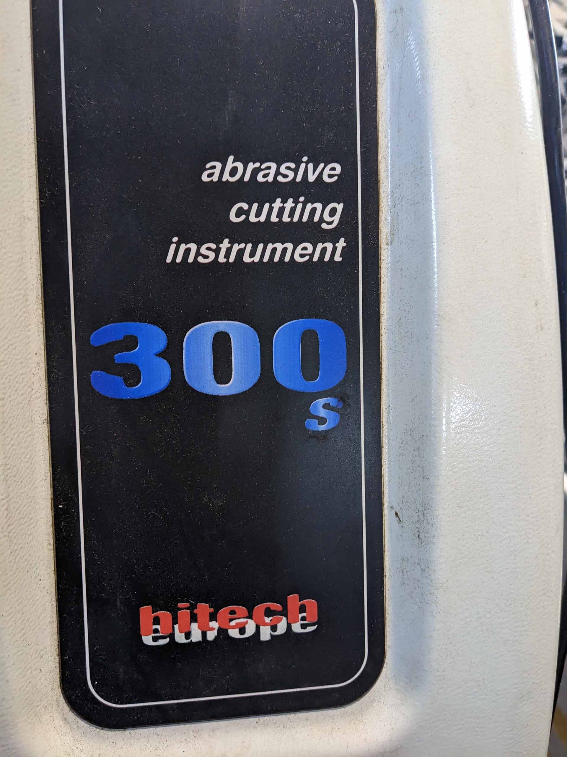
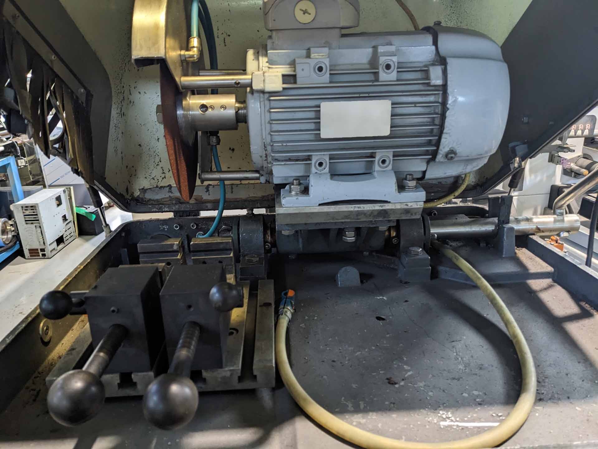
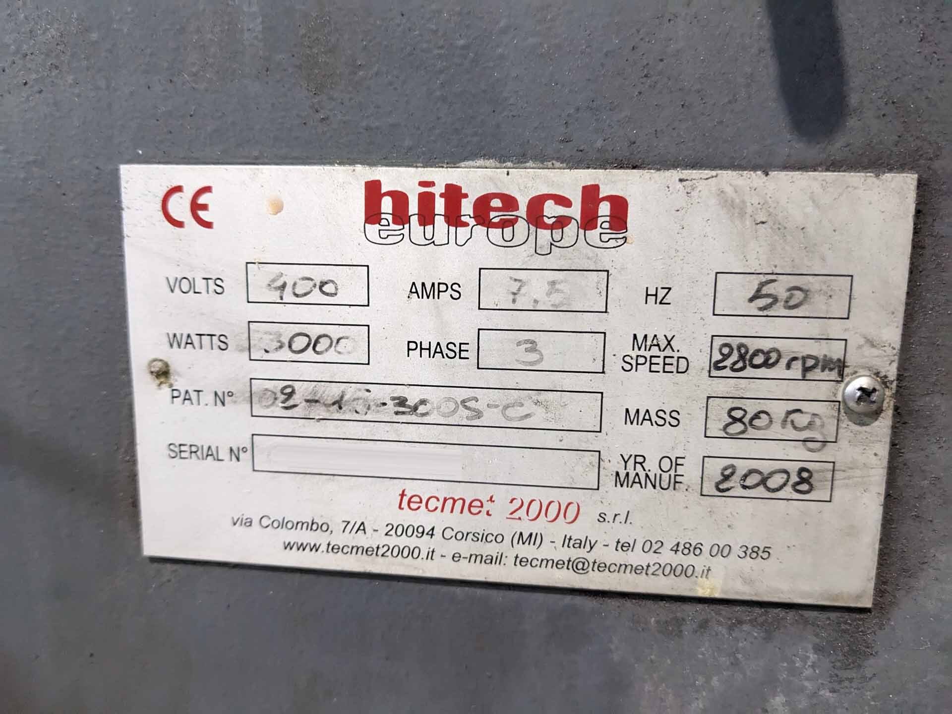
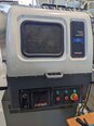
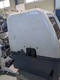
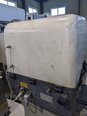
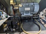
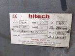
HITECH 300S / Tecmet 2000 wafer grinding, lapping, and polishing equipment is a cutting-edge and technologically advanced equipment designed for precision surface finishing of semiconductor wafers used in the fabrication of integrated circuits (ICs). This system offers a comprehensive solution for achieving sub-micron level flatness, surface roughness, and thickness uniformity on wafers, crucial for ensuring the optimal performance of semiconductor devices. At the core of 300S / Tecmet 2000 unit is a robust and highly efficient grinding, lapping, and polishing mechanism that utilizes advanced abrasive materials and precision machining technologies to achieve superior wafer surface processing results. The machine integrates multiple processing steps into a single platform, providing a seamless workflow for wafer thinning, flattening, and polishing with high throughput and repeatability. One of the key features of HITECH 300S / Tecmet 2000 tool is its high-precision control asset that enables users to customize and fine-tune the processing parameters according to specific application requirements. The model offers a wide range of adjustable parameters such as grinding pressure, rotation speed, abrasive particle size, and process time, allowing operators to optimize the processing conditions for different wafer materials and sizes. 300S / Tecmet 2000 equipment is equipped with advanced automation capabilities, including robotic wafer handling and intelligent process control software, which ensures consistent and reproducible results across multiple processing cycles. The system can also be integrated with in-line metrology tools for real-time monitoring of wafer thickness, flatness, and surface roughness, enabling on-the-fly adjustments to maximize processing efficiency and yield. In terms of performance, HITECH 300S / Tecmet 2000 unit excels in achieving ultra-flat wafer surfaces with sub-micron level roughness and thickness uniformity, meeting the stringent requirements of modern semiconductor manufacturing processes. The machine is capable of processing a wide range of wafer materials including silicon, gallium arsenide, and sapphire, with thicknesses ranging from a few microns to several hundred microns. 300S / Tecmet 2000 tool is designed with versatility in mind, accommodating various wafer sizes up to 300mm in diameter and offering a range of compatible tooling options for different processing applications. The asset's modular design allows for easy maintenance and upgrades, ensuring long-term reliability and performance consistency in demanding semiconductor production environments. Overall, HITECH 300S / Tecmet 2000 wafer grinding, lapping, and polishing model represents a state-of-the-art solution for achieving high-precision surface finishing of semiconductor wafers, enabling semiconductor manufacturers to meet the ever-increasing demands for advanced IC devices with superior performance and reliability. By leveraging the equipment's advanced capabilities and automation features, semiconductor companies can streamline their wafer processing workflows, improve production efficiency, and deliver high-quality semiconductor products to the market.
There are no reviews yet