Used ASML 5000/55 #293827875 for sale
URL successfully copied!
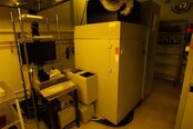
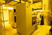
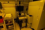
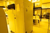
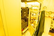
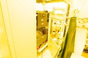
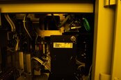
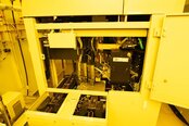
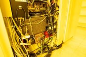
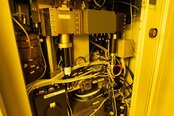
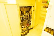

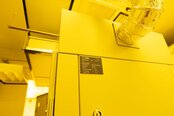


Tap to zoom

ID: 293827875
Wafer Size: 4"-6"
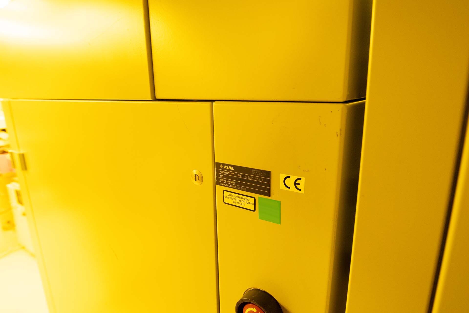
Vintage: 2002
Steppers, 4"-6"
Silicon Carbide (Sic)
2002 vintage.
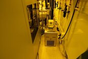
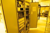
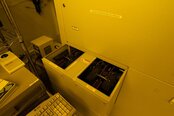
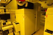
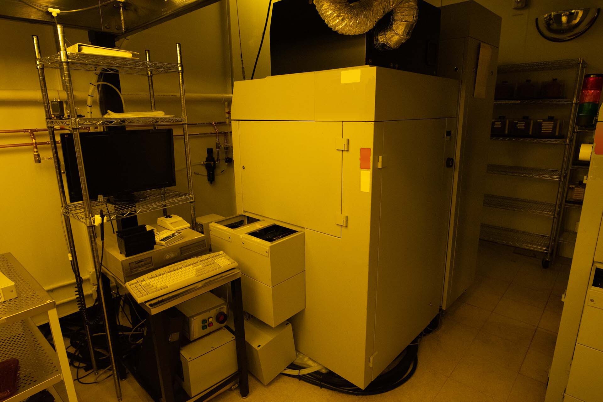
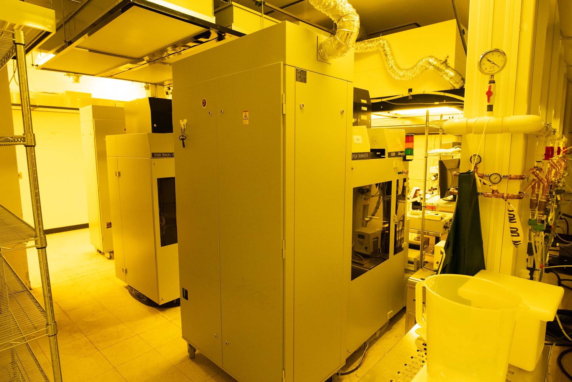
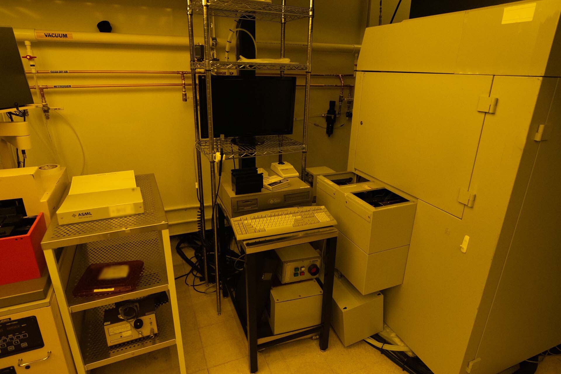
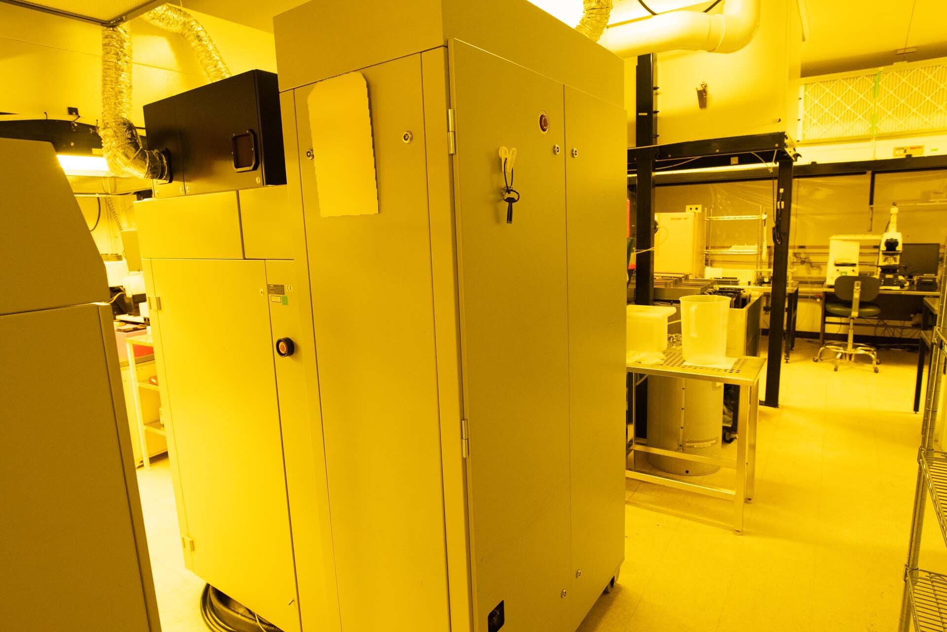
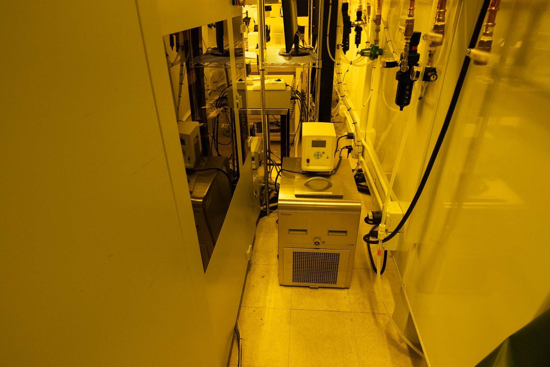
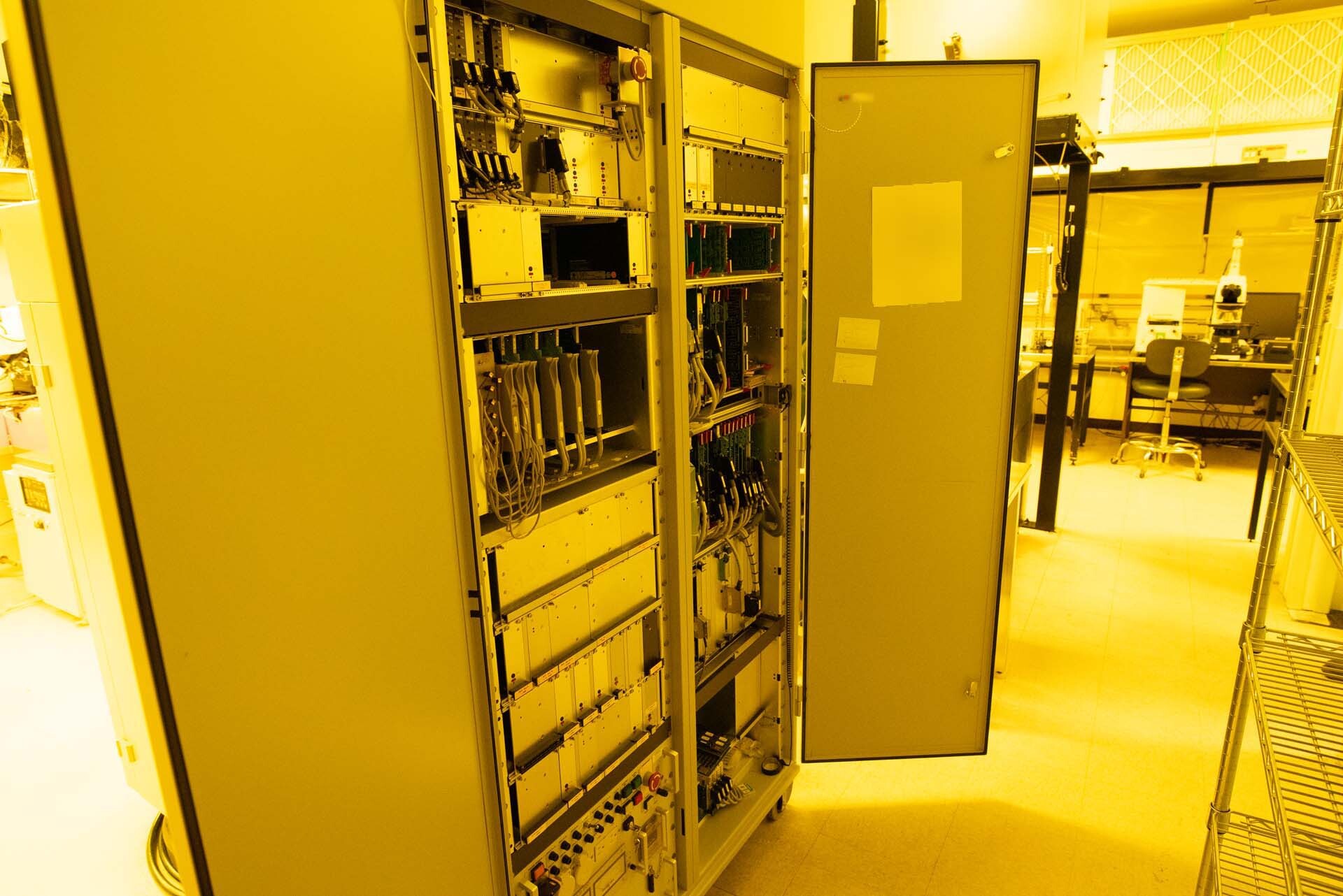
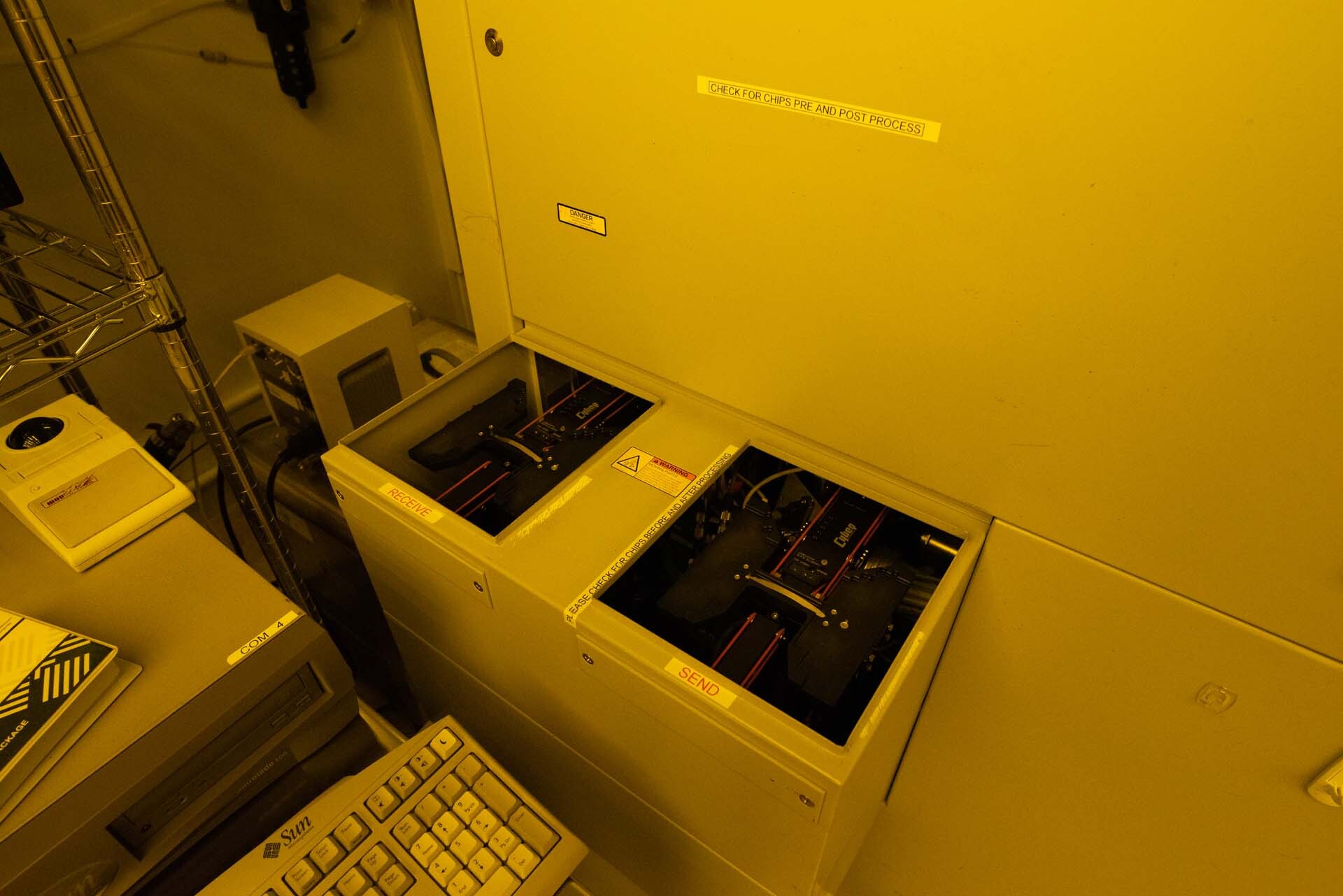
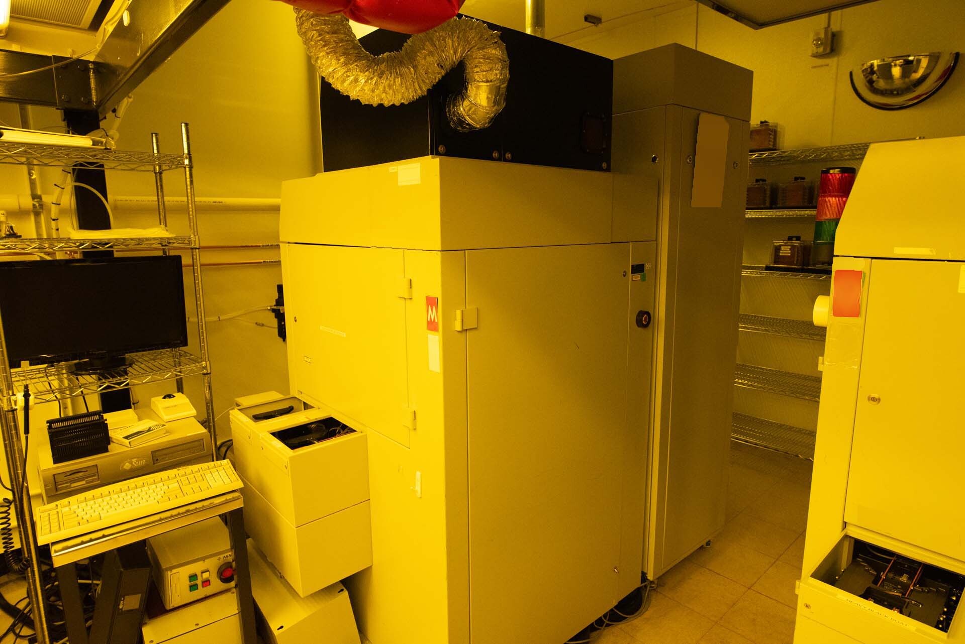
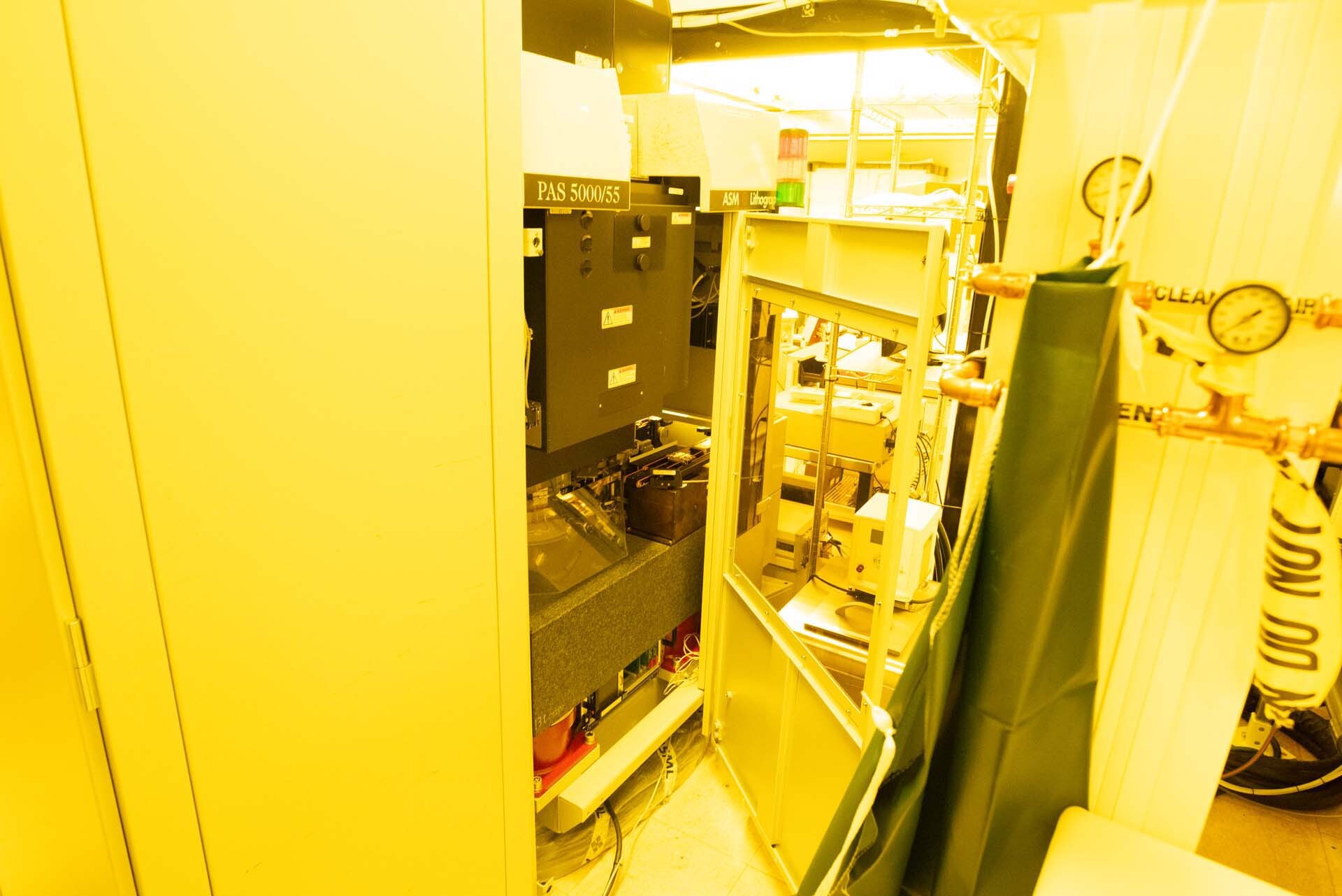
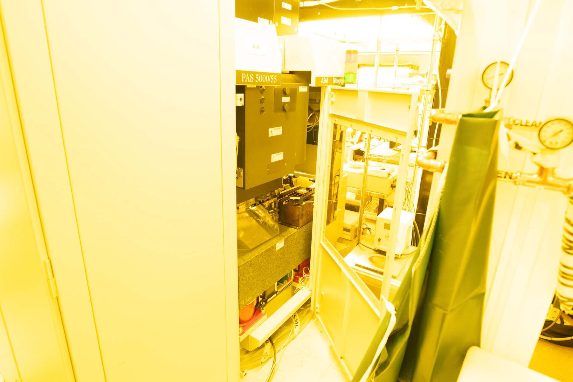
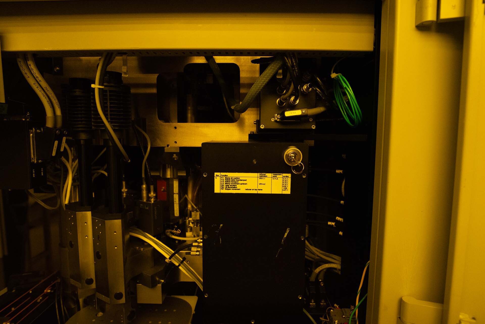
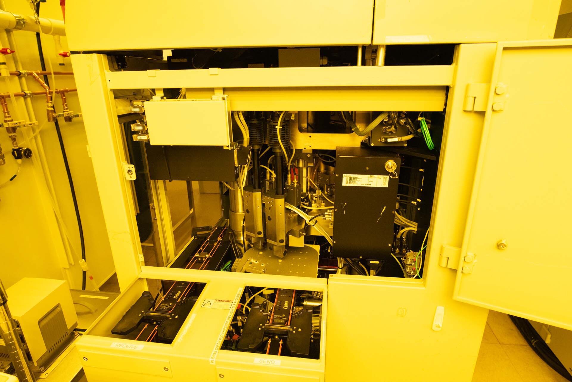
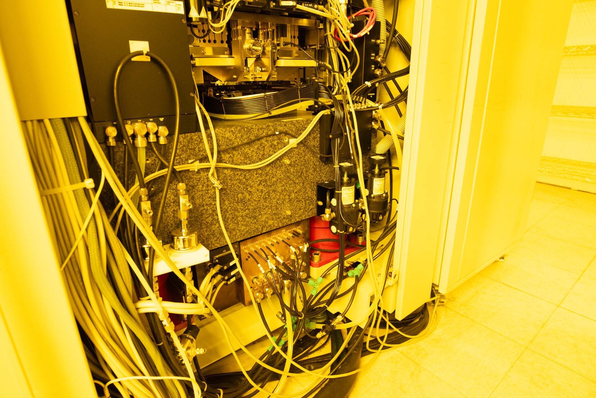
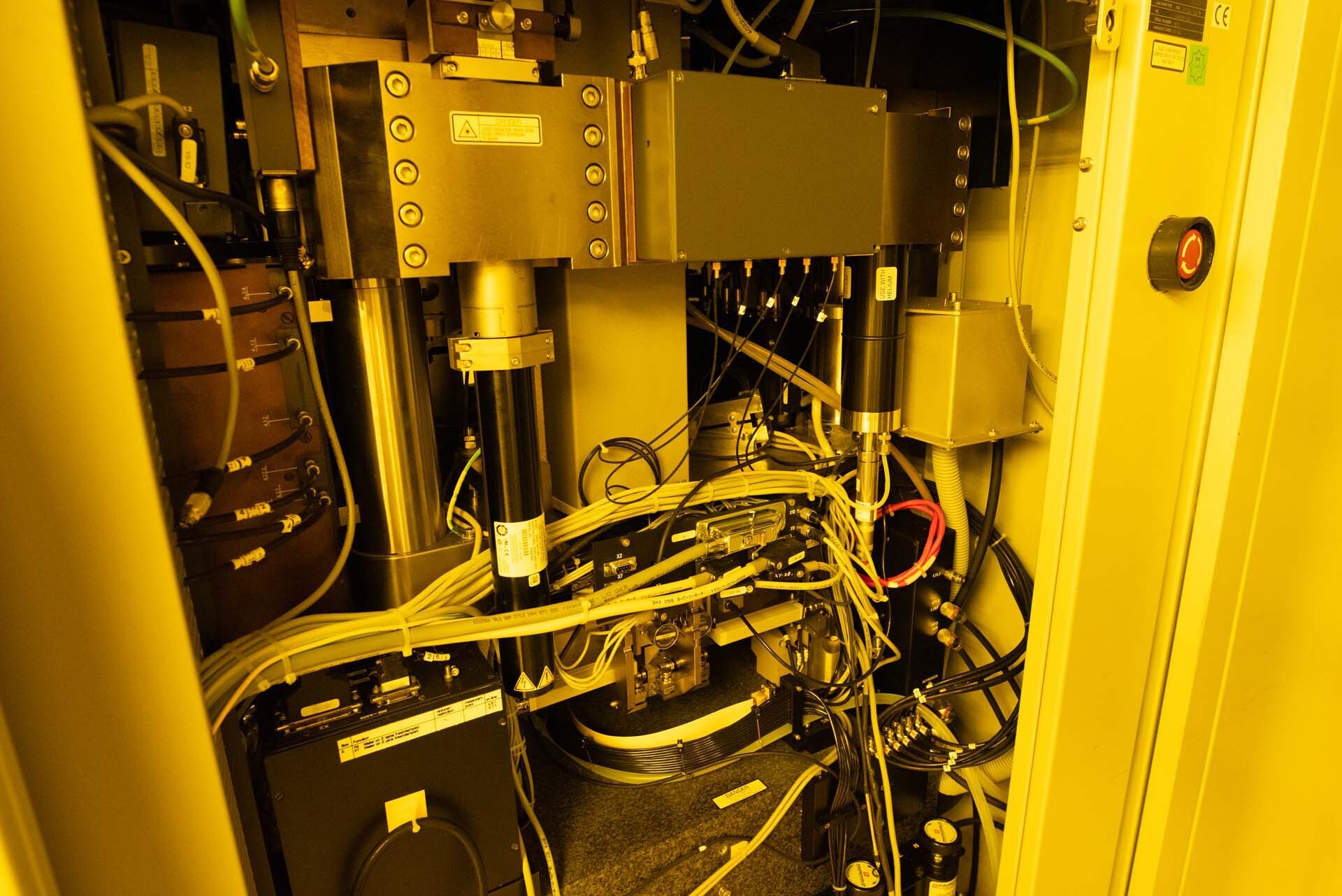
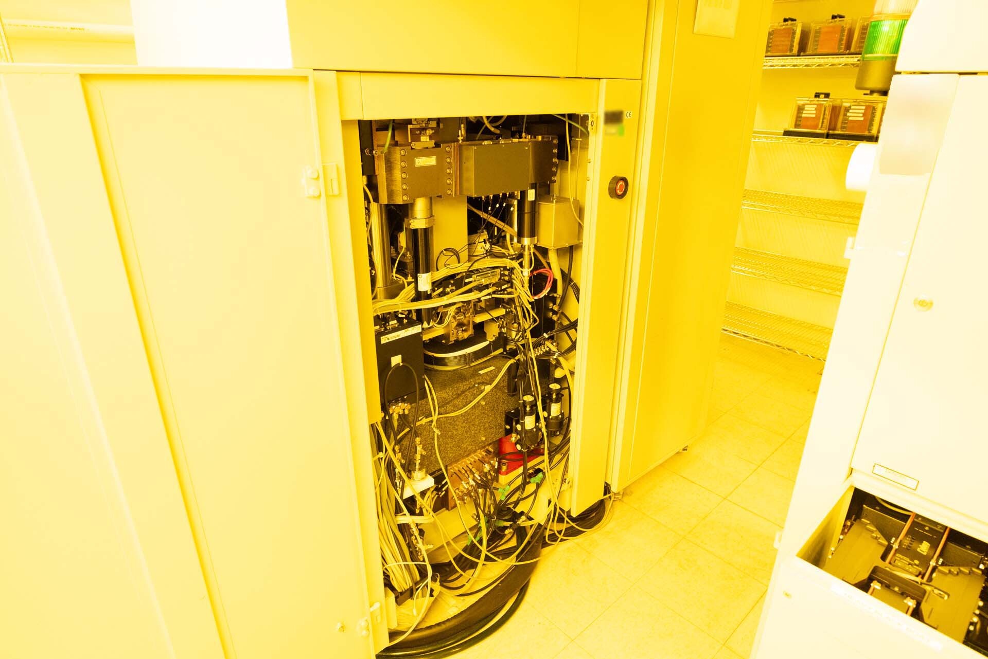
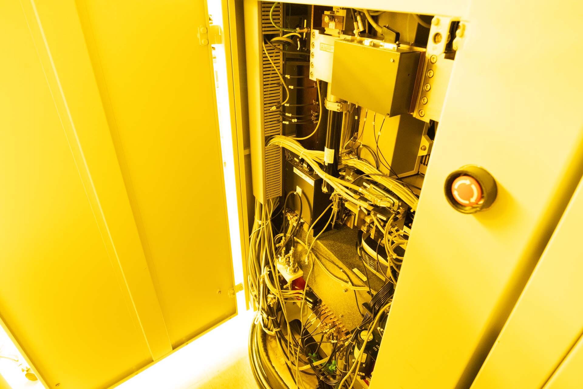
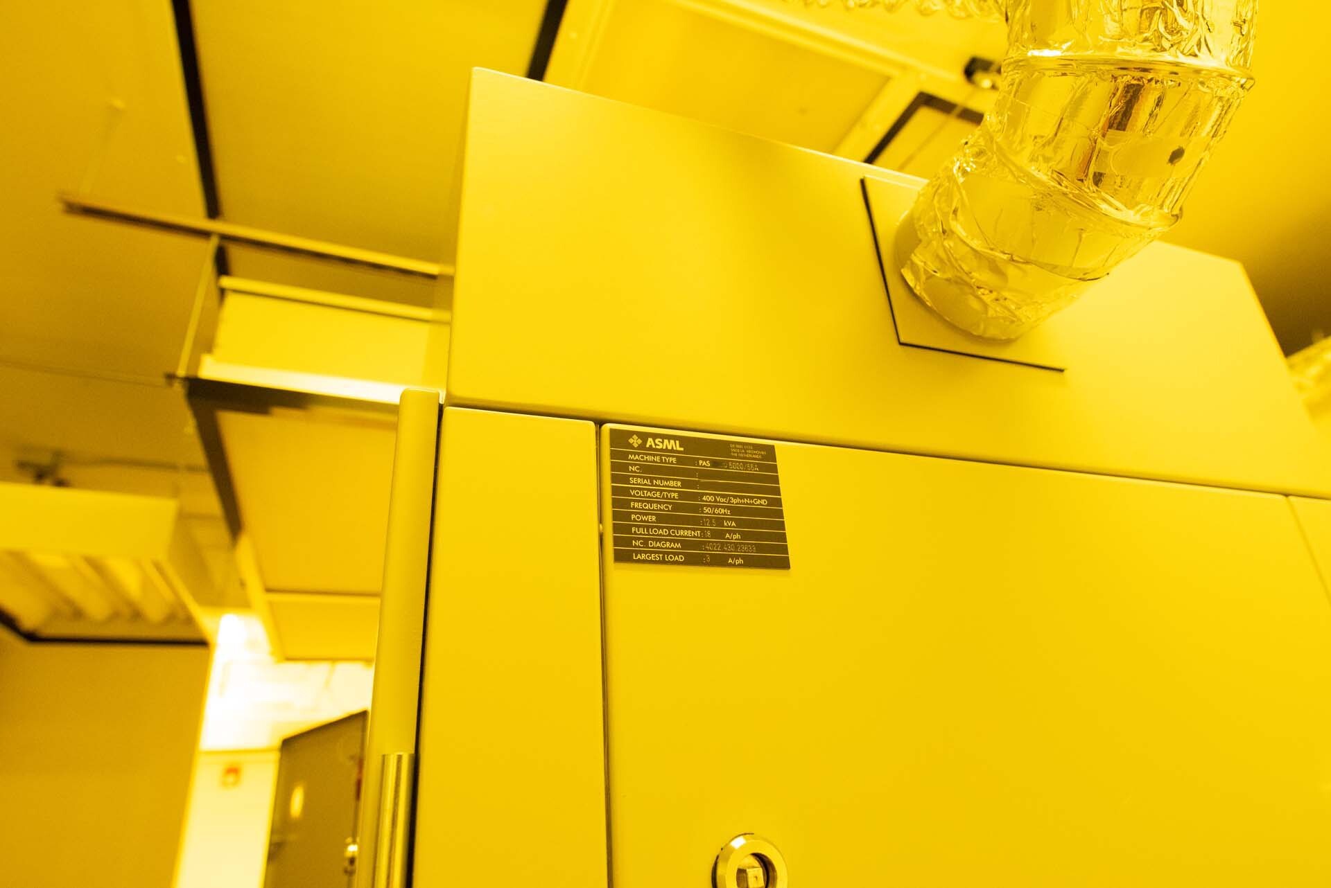
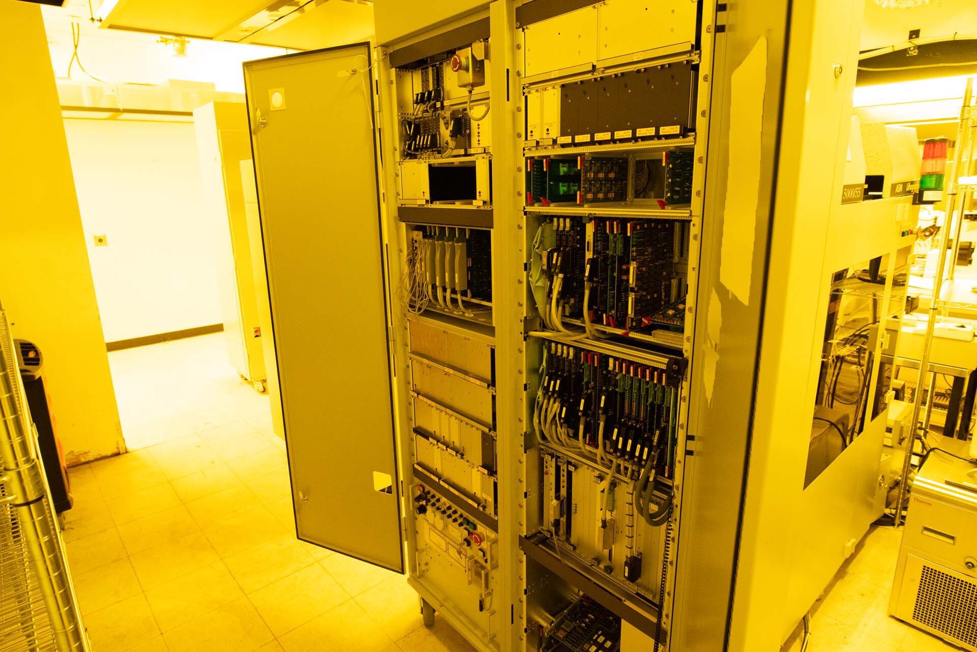
ASML 5000/55 is a state-of-the-art wafer stepper that plays a crucial role in the semiconductor manufacturing process. This advanced photolithography equipment is designed and manufactured by ASML, a leading supplier of photolithography systems for the semiconductor industry. ASML 5000 / 55 is renowned for its precision, speed, and reliability, making it a preferred choice for leading semiconductor manufacturers worldwide. At the heart of 5000/55 is a sophisticated optics system that enables the precise patterning of semiconductor wafers. The stepper uses a process known as photolithography to transfer patterns from a mask onto a wafer. This step is critical in the fabrication of integrated circuits, where intricate patterns need to be accurately replicated on silicon substrates to create functional electronic devices. 5000 / 55 is equipped with a powerful light source, typically using deep ultraviolet (DUV) light in the range of 248nm or 193nm. This short wavelength light is essential for achieving high resolution and allows for the production of small features on the wafer. The stepper also features a sophisticated lens unit that can precisely focus the light onto the wafer, ensuring accurate pattern transfer. One of the key features of ASML 5000/55 is its stepper stage, which provides precise positioning and movement of the wafer during exposure. The stepper stage allows for fine adjustments to align the wafer with the mask pattern, ensuring that patterns are accurately transferred with sub-micron precision. This level of precision is critical for producing the complex and densely packed circuits found in modern semiconductor devices. ASML 5000 / 55 is also equipped with advanced alignment and calibration systems that ensure the accurate registration of the mask and wafer layers. Through sophisticated feedback mechanisms and algorithms, the stepper can detect and correct for any misalignments or distortions, ensuring high yield and uniformity across wafers. This level of precision and automation reduces production variability and improves overall process control. Furthermore, 5000/55 features an advanced wafer handling machine that enables seamless loading and unloading of wafers during the exposure process. The tool is designed to minimize contamination and ensure the integrity of the wafers throughout the manufacturing process. This automation not only improves throughput but also enhances the overall yield and reliability of the semiconductor manufacturing process. In addition to its technical capabilities, 5000 / 55 is designed for high productivity and efficiency. The stepper is capable of processing a large number of wafers per hour, making it ideal for high-volume semiconductor production facilities. The asset is also known for its reliability, with a robust design that minimizes downtime and maintenance requirements. Overall, ASML 5000/55 represents the cutting edge of photolithography technology in the semiconductor industry. Its precision, speed, and reliability make it an essential tool for manufacturing the advanced semiconductor devices that power modern electronics. As semiconductor technology continues to advance, ASML 5000 / 55 remains a key enabler for pushing the boundaries of device miniaturization and performance.
There are no reviews yet