Used ASML 5000/55 #293827997 for sale
URL successfully copied!
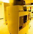
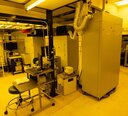

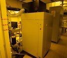

Tap to zoom
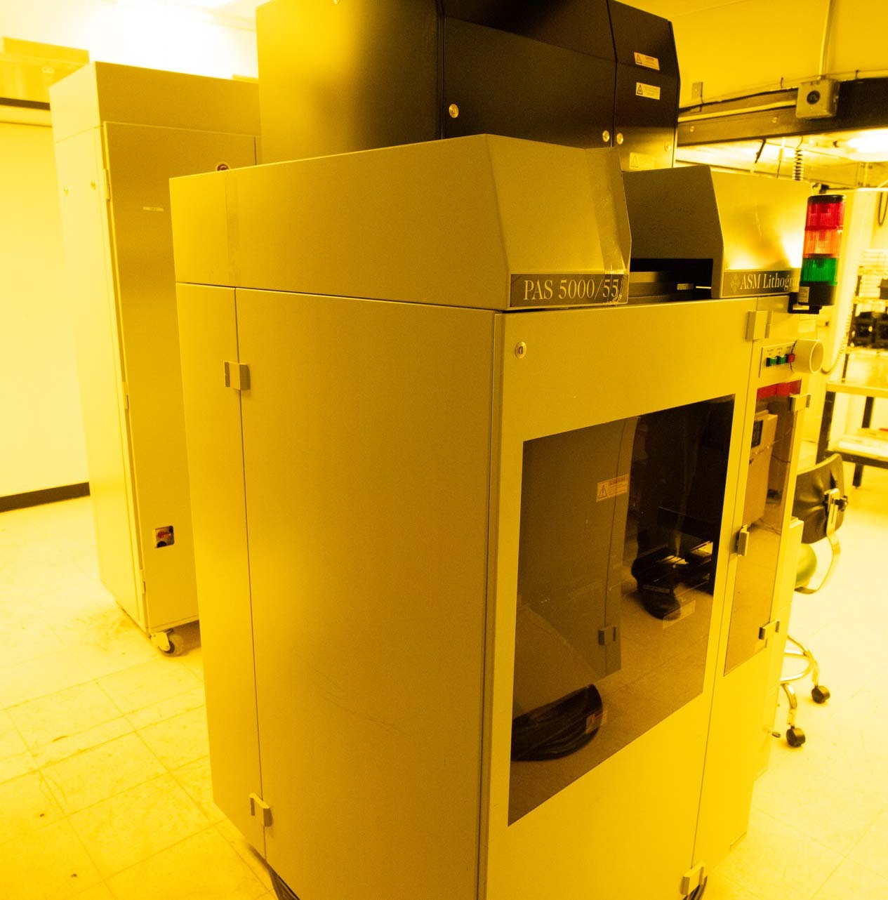

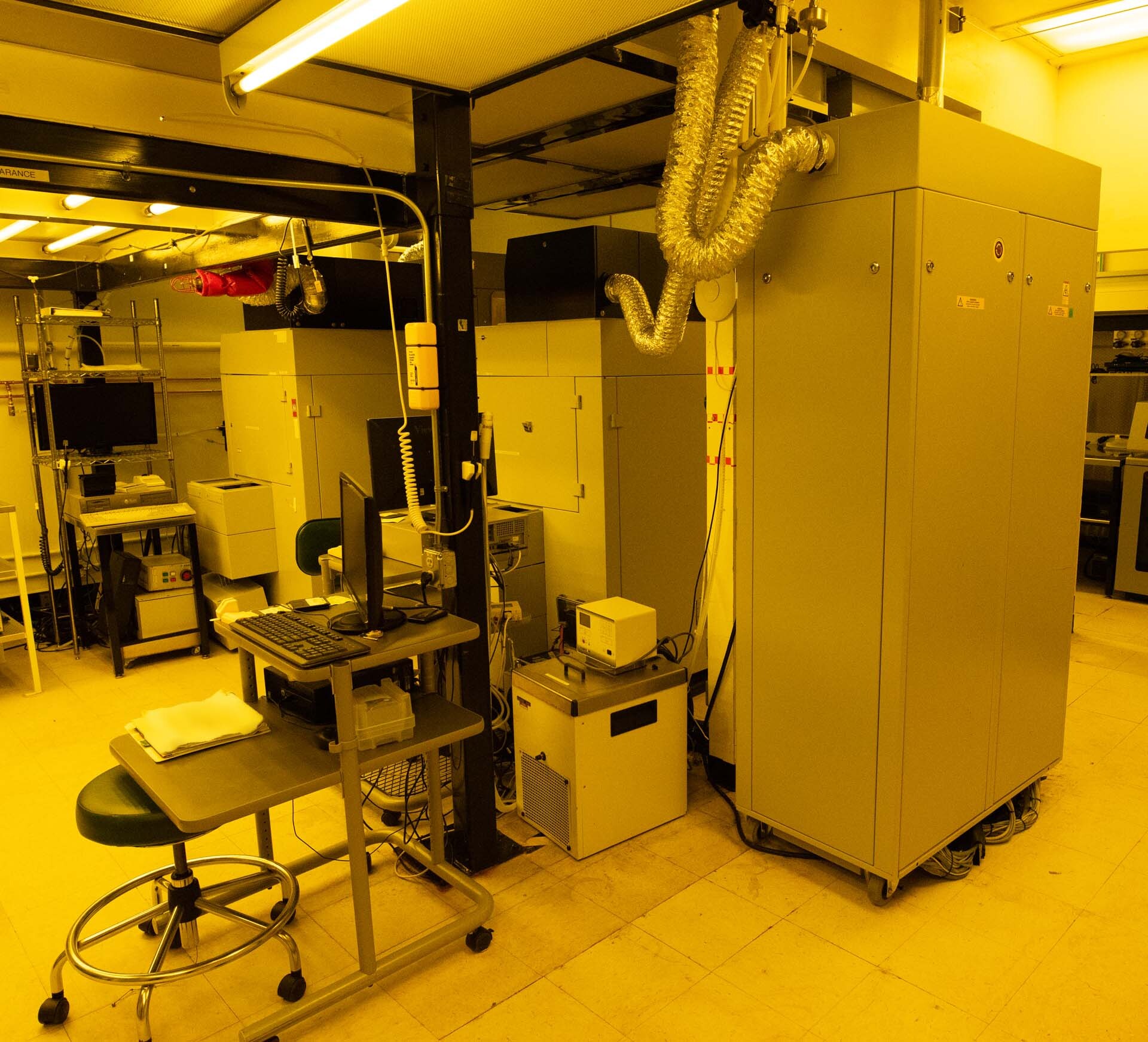
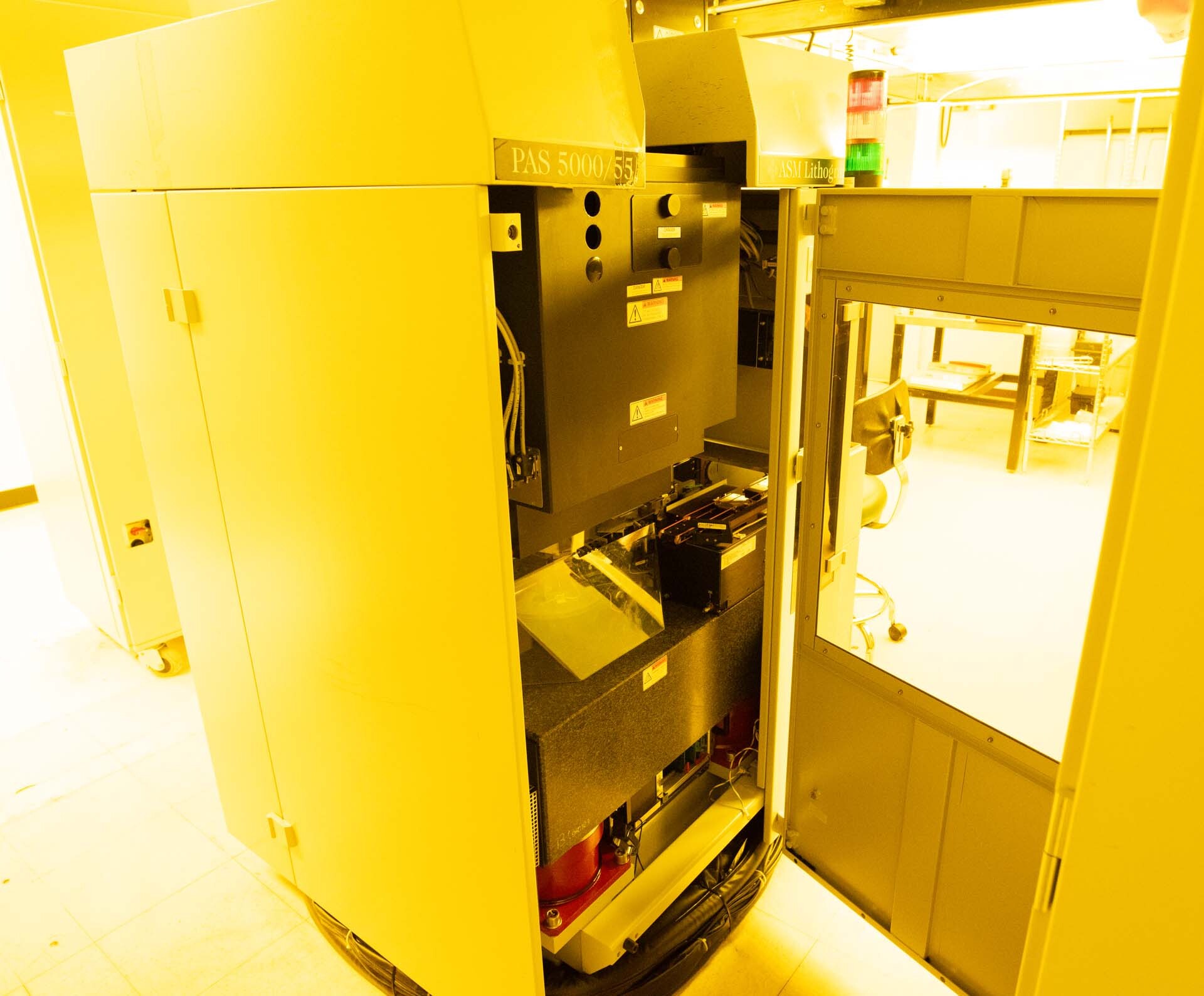
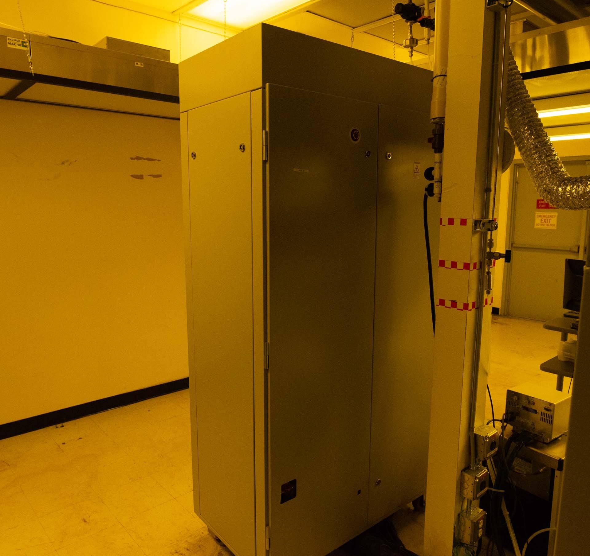
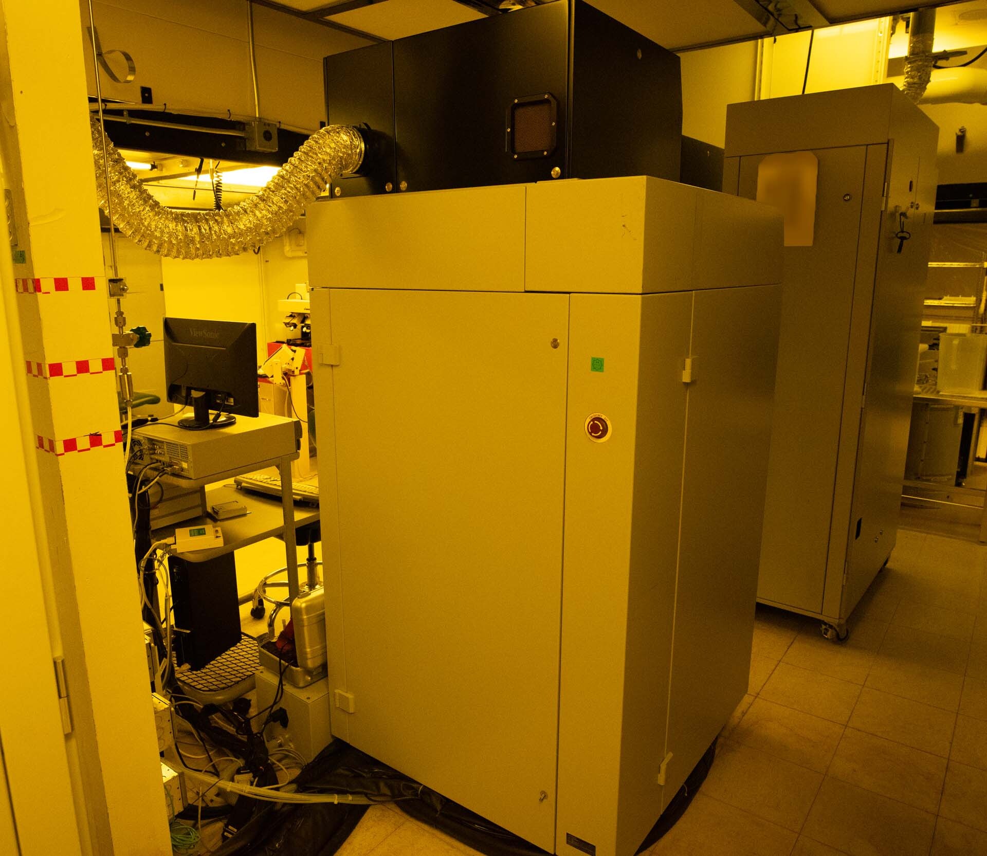
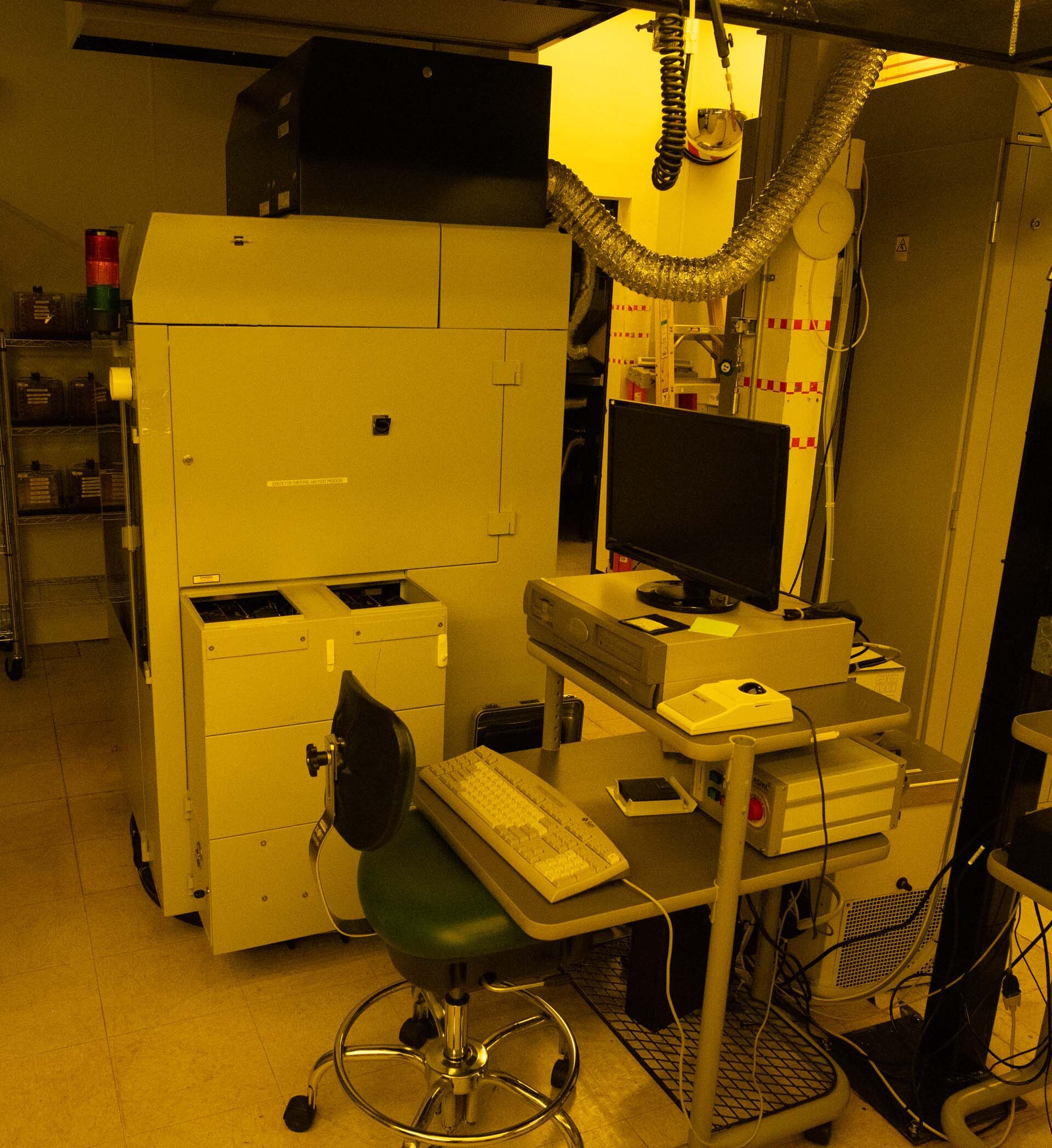
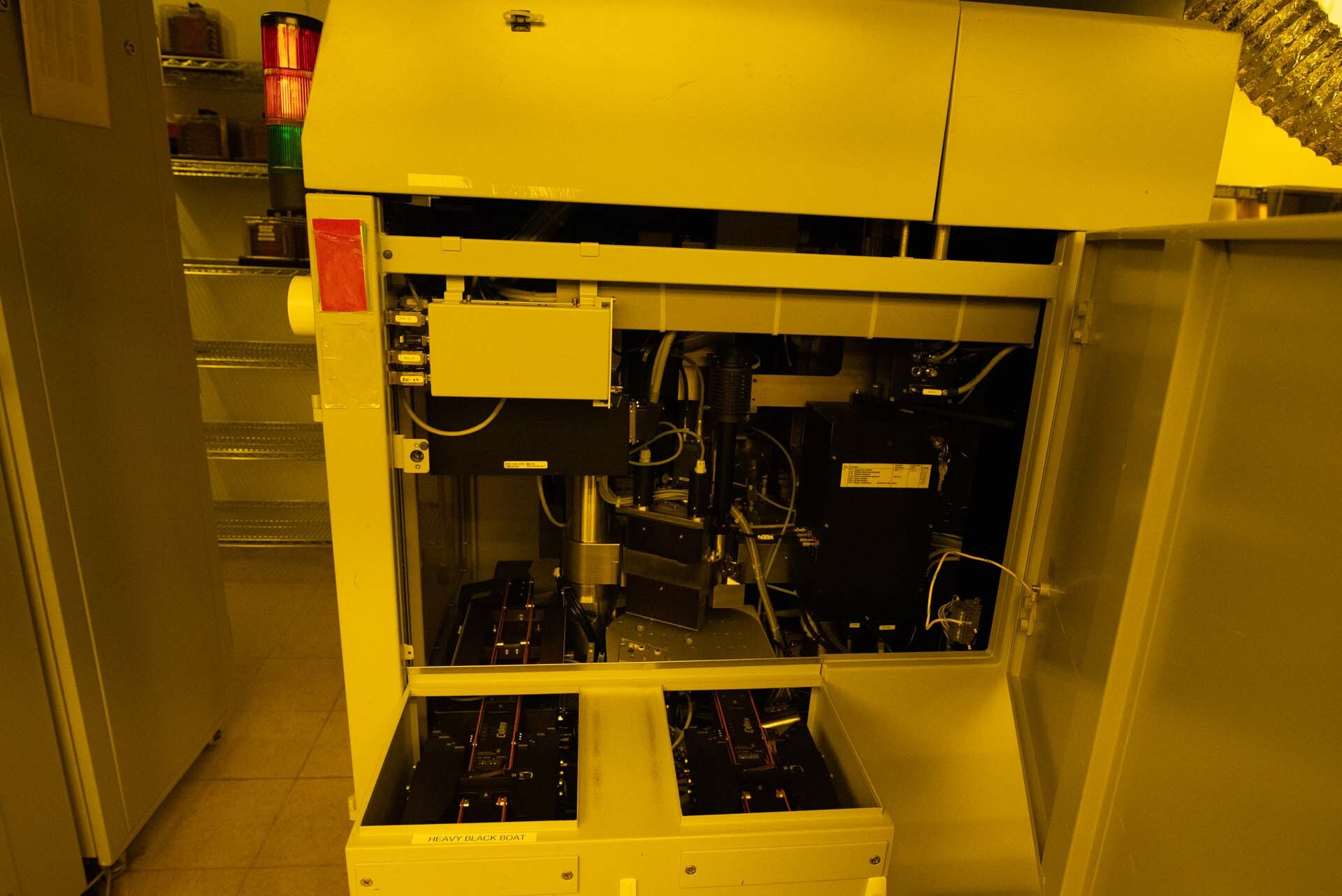
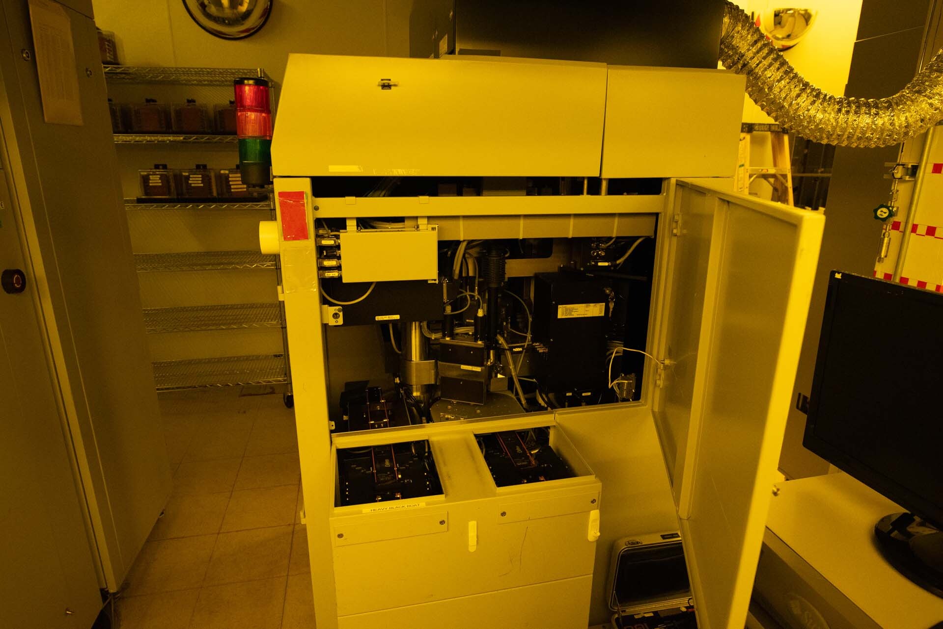
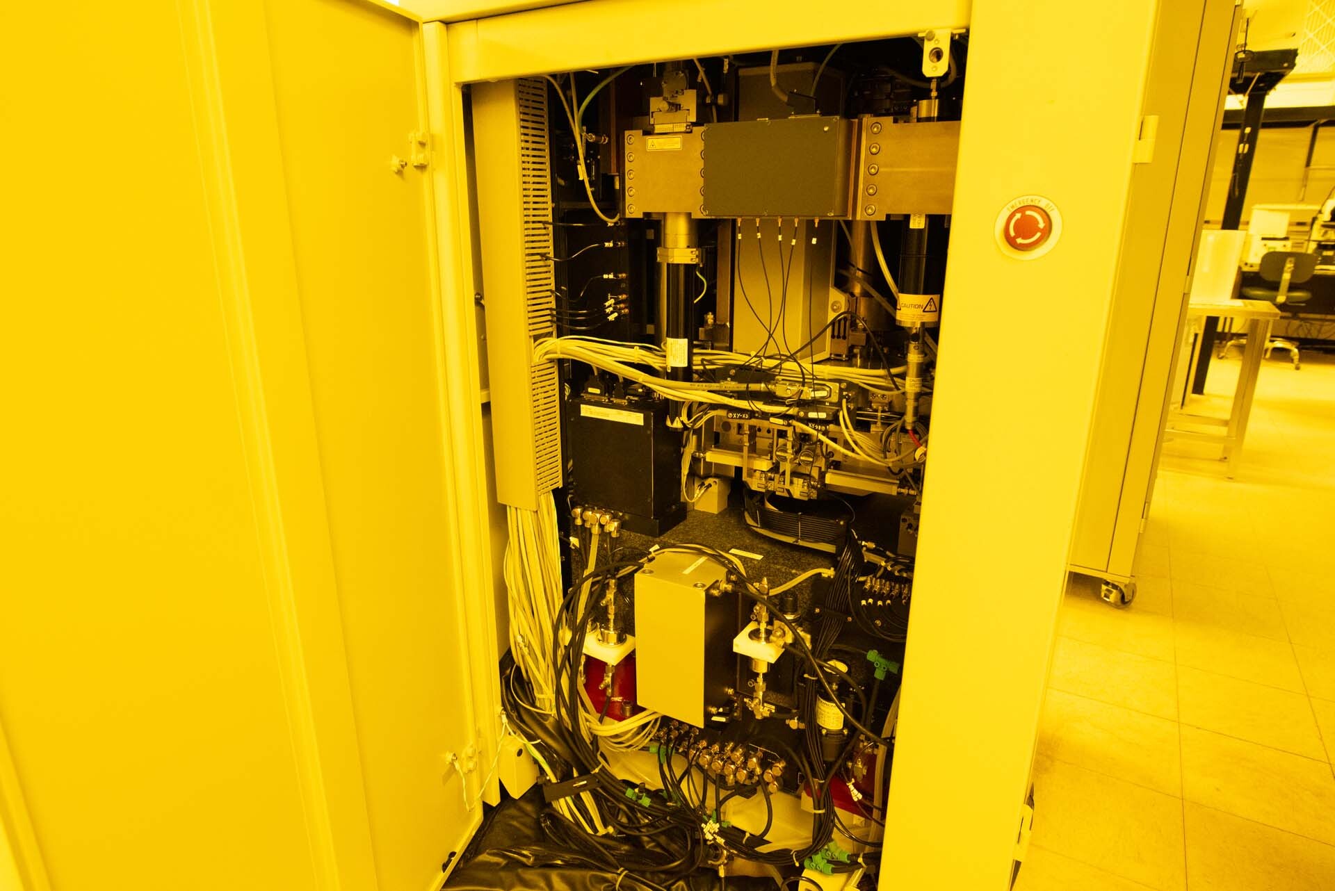
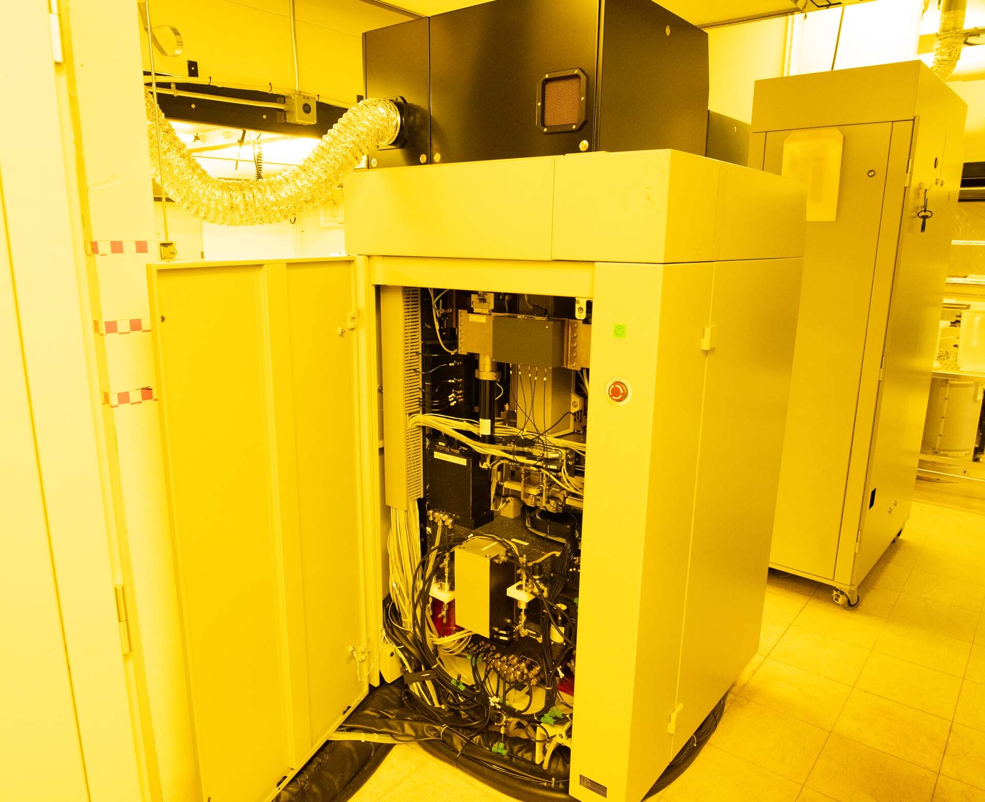
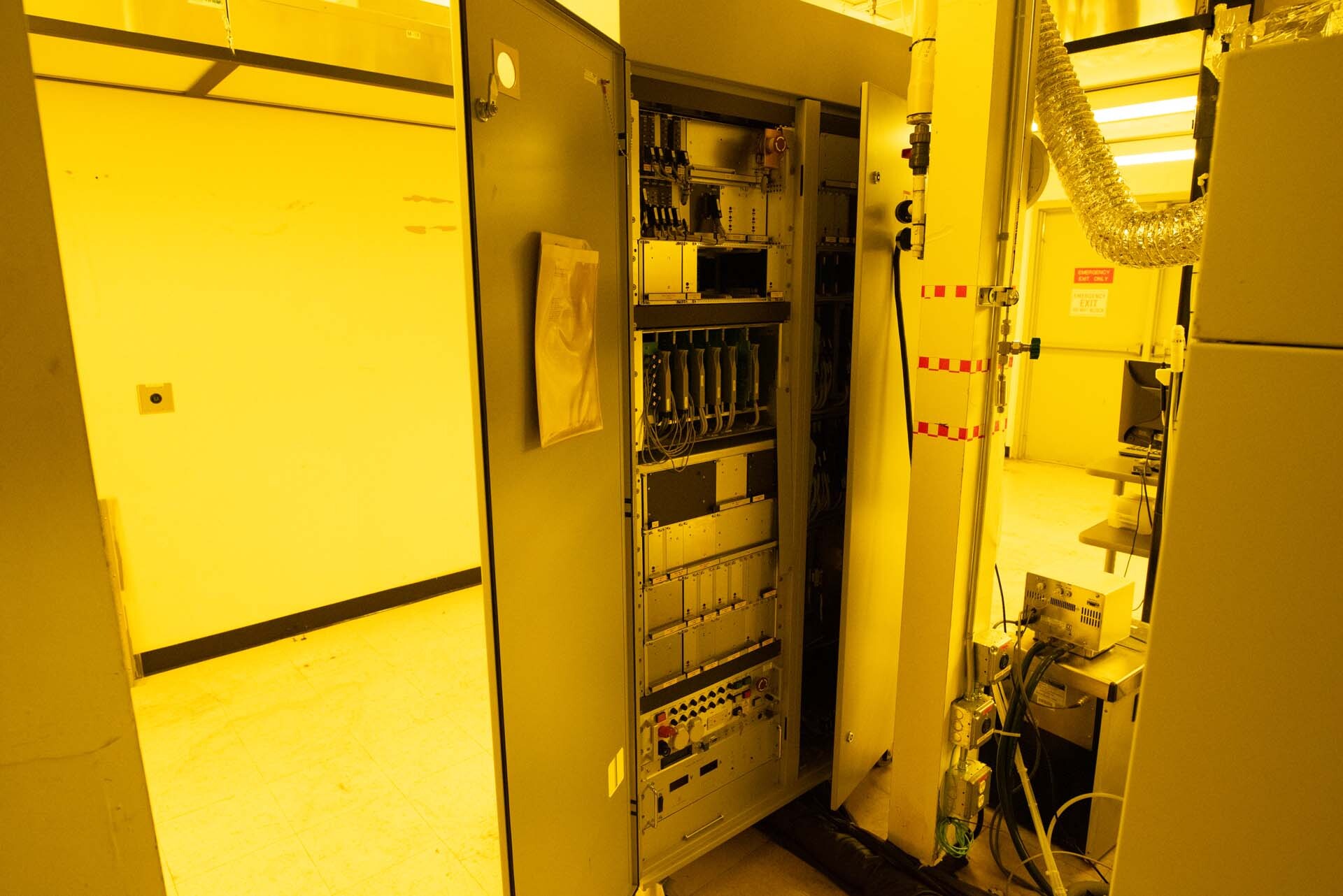
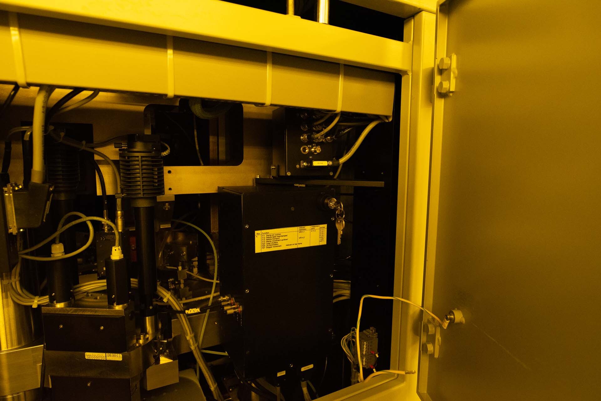
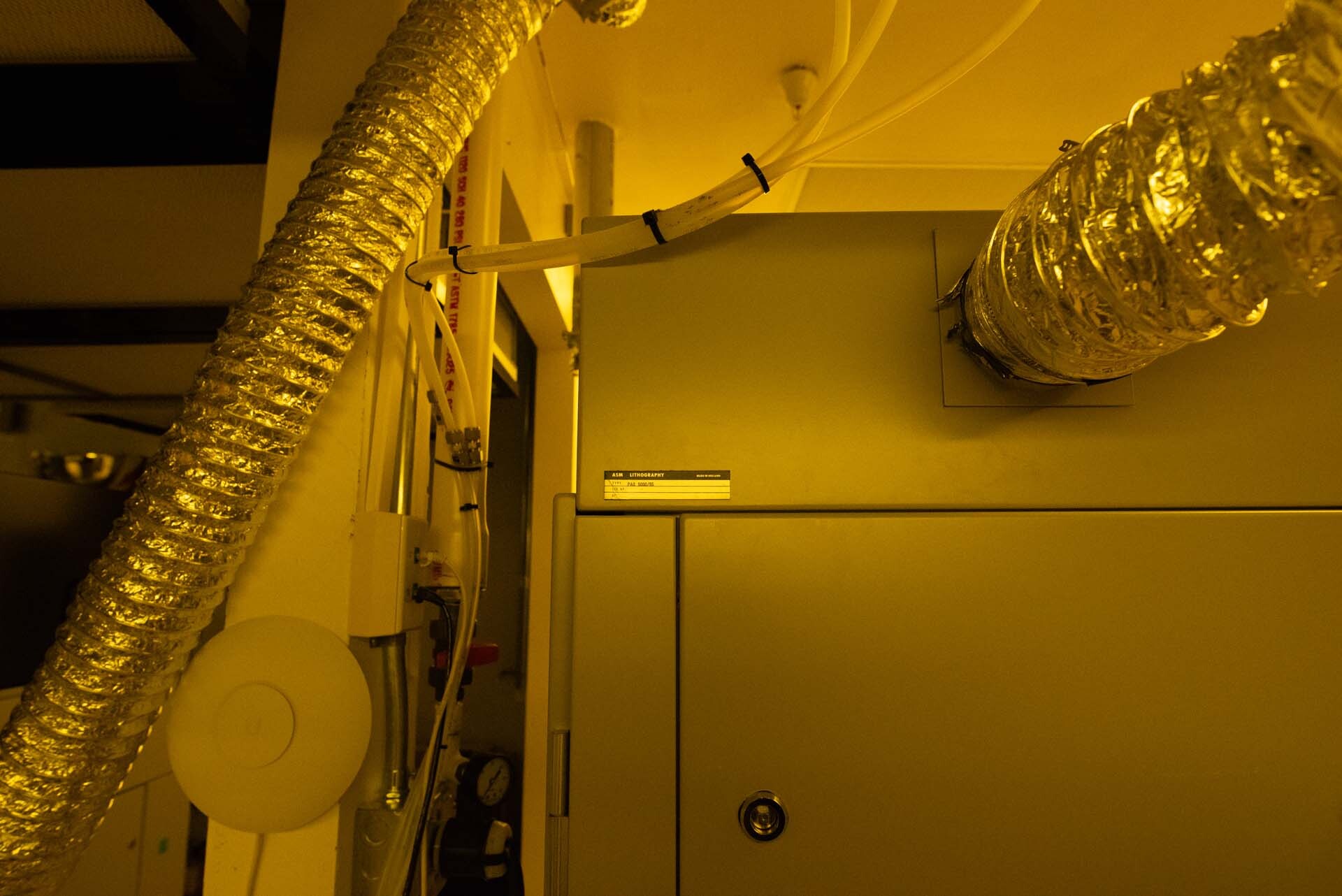
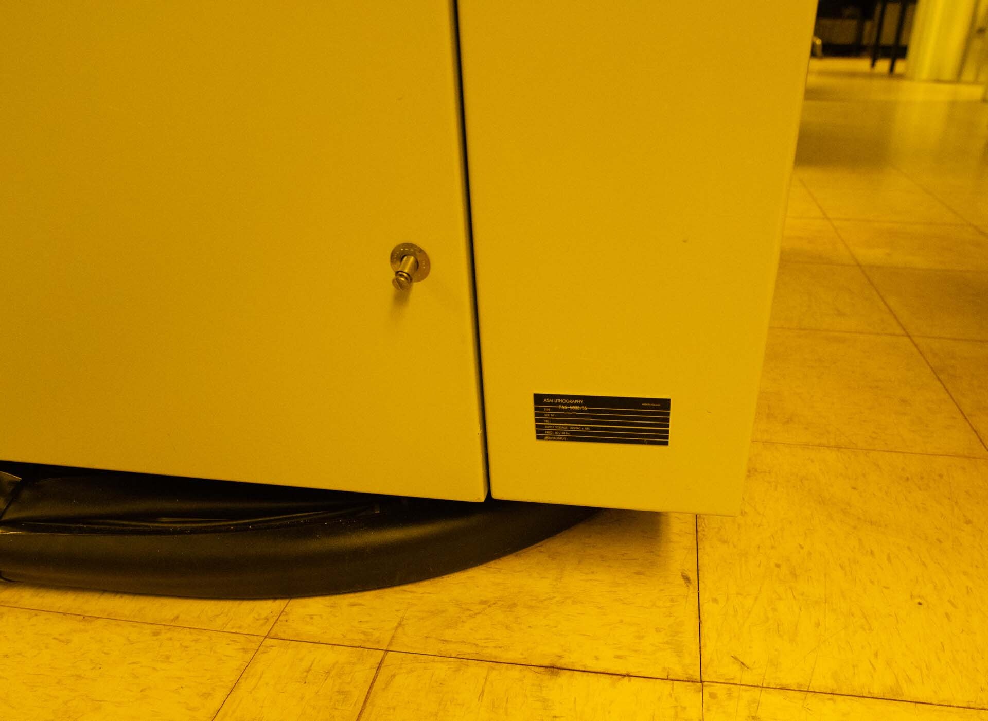
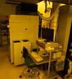
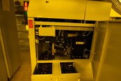
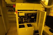
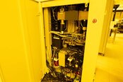
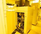
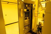
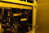
ASML 5000/55 is a sophisticated wafer stepper equipment utilized in semiconductor manufacturing processes for precise photolithography. It plays a crucial role in patterning integrated circuits on silicon wafers with exceptional accuracy and resolution. Developed by ASML, a leading provider of photolithography equipment, ASML 5000 / 55 is renowned for its advanced technology, reliability, and performance in the semiconductor industry. 5000/55 operates based on the principle of photolithography, a process that involves transferring a pattern from a photomask onto a semiconductor wafer coated with a light-sensitive photoresist material. This system employs a high-energy light source, typically a deep ultraviolet (DUV) laser, to expose the photoresist on the wafer, defining the circuit pattern with extreme precision. The stepper moves the wafer and the photomask in a synchronized manner, allowing for the accurate replication of the mask pattern onto the wafer surface. One of the key features of 5000 / 55 is its advanced projection lens unit, which is essential for achieving the required resolution and critical dimension control in semiconductor patterning. The projection lens focuses the light from the laser onto the wafer surface, enabling the creation of fine geometric features on the integrated circuits. With a high numerical aperture and low aberration levels, the projection lens of ASML 5000/55 ensures sharp and accurate imaging of the mask pattern onto the wafer with minimal distortion. ASML 5000 / 55 is equipped with a sophisticated alignment and overlay control machine to ensure proper registration of multiple layers of patterns on the wafer. Through the use of precision alignment marks and feedback mechanisms, the tool can align each exposure accurately with the previously patterned layers, maintaining the desired overlay accuracy for complex chip designs. This capability is crucial for achieving tight tolerances and minimizing defects in the final semiconductor devices. In terms of throughput and productivity, 5000/55 offers high-speed wafer processing capabilities to meet the demanding production requirements of semiconductor fabrication facilities. With advanced automation features, such as robotic wafer handling systems and software-controlled process sequences, the asset can achieve rapid exposure and patterning of wafers while maintaining consistent quality and uniformity across the wafer surface. Moreover, 5000 / 55 is designed for scalability and flexibility to accommodate various semiconductor fabrication processes and technology nodes. The model supports a wide range of wafer sizes, from small diameters used in research and development to large diameters for high-volume production. Additionally, it is compatible with different types of photoresist materials, exposure wavelengths, and resolution requirements, allowing semiconductor manufacturers to adapt the equipment to their specific process needs. Overall, ASML 5000/55 represents a cutting-edge solution for semiconductor lithography, combining precision optics, advanced automation, and high-speed processing capabilities to enable the production of advanced integrated circuits with exceptional quality and performance. With its reliability, performance, and flexibility, this wafer stepper system continues to be a preferred choice for leading semiconductor manufacturers worldwide seeking to push the boundaries of technology and innovation in the semiconductor industry.
There are no reviews yet