Used ASML AT-850C #9256716 for sale
URL successfully copied!
Tap to zoom


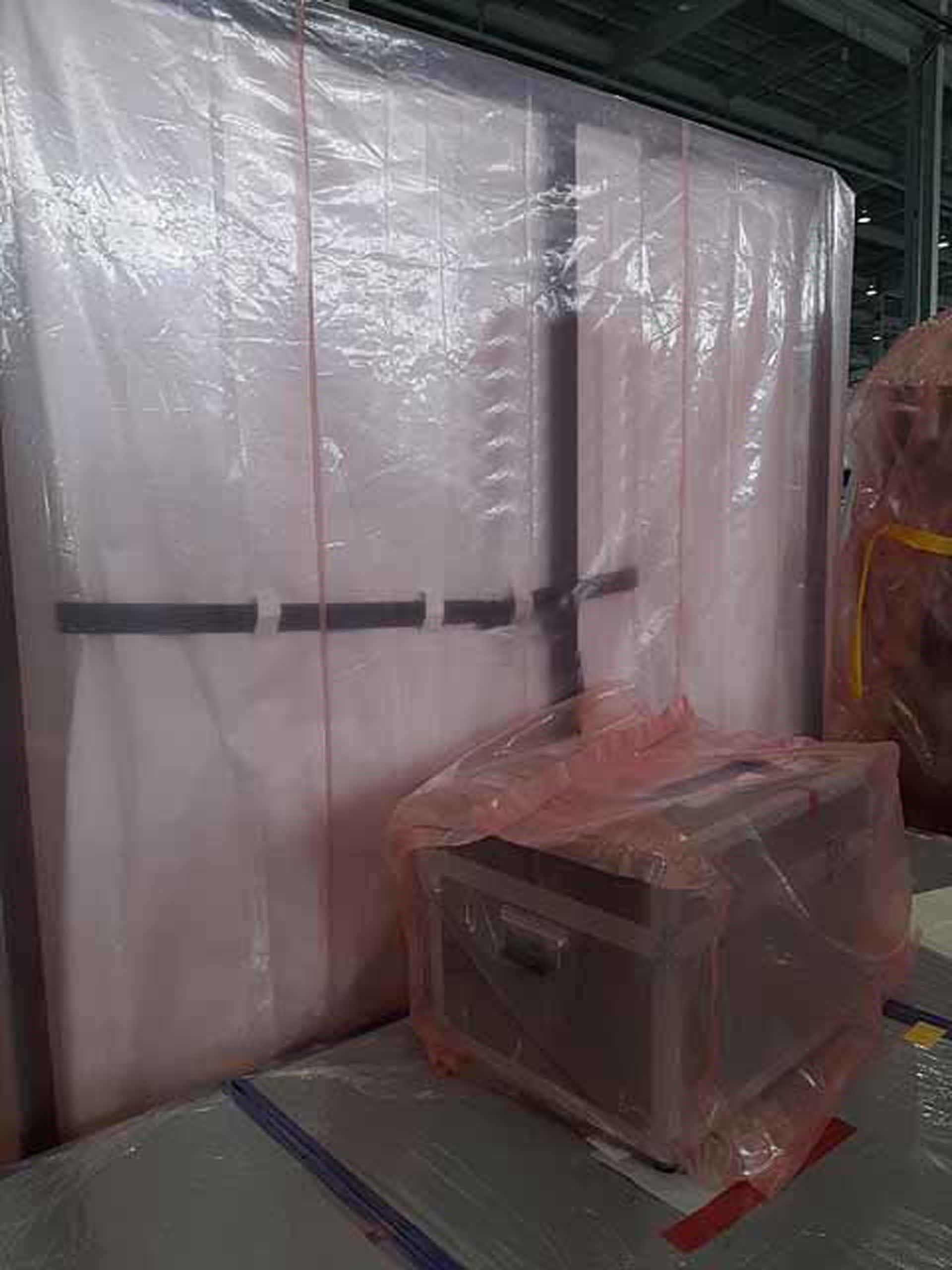

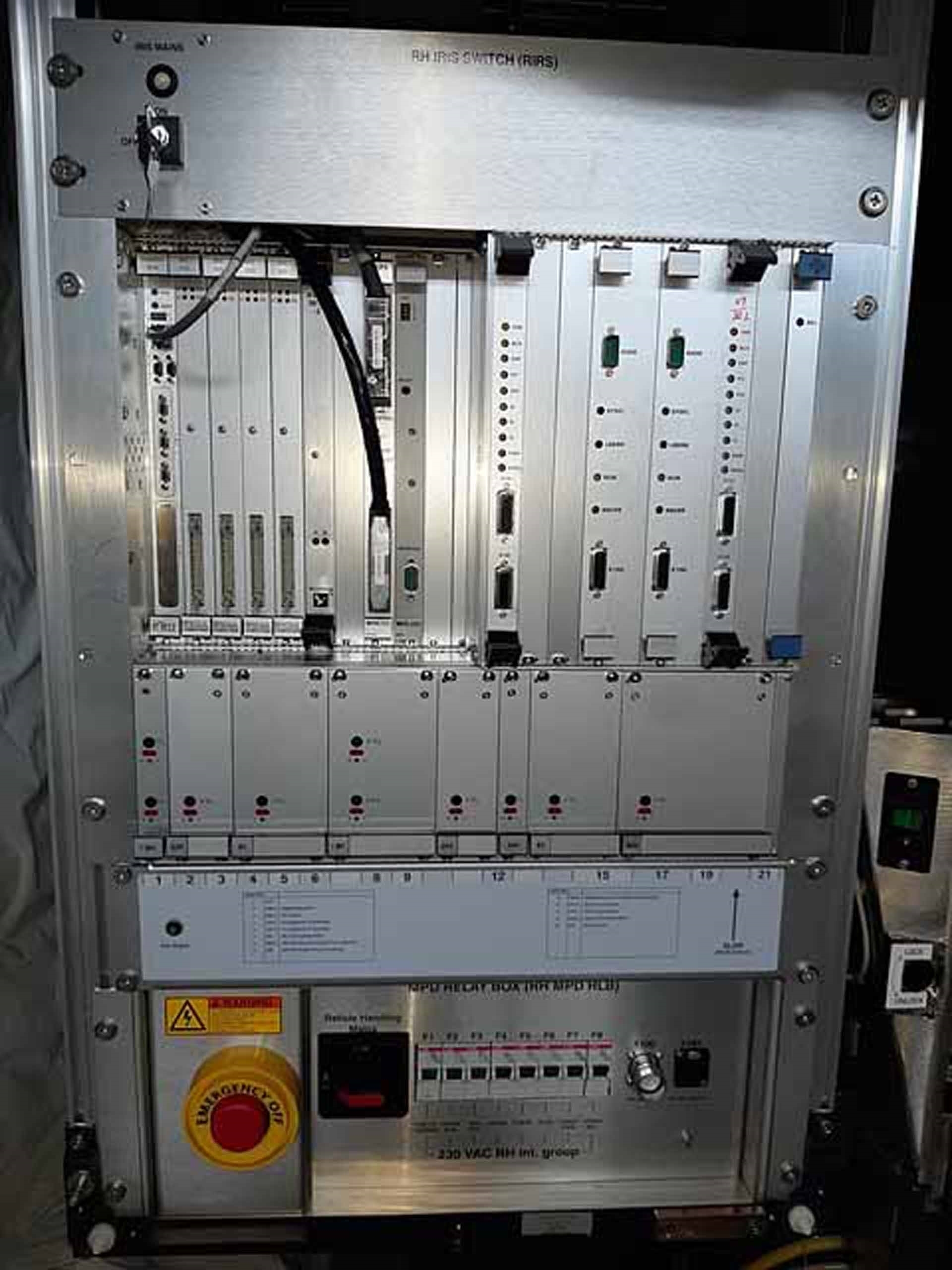


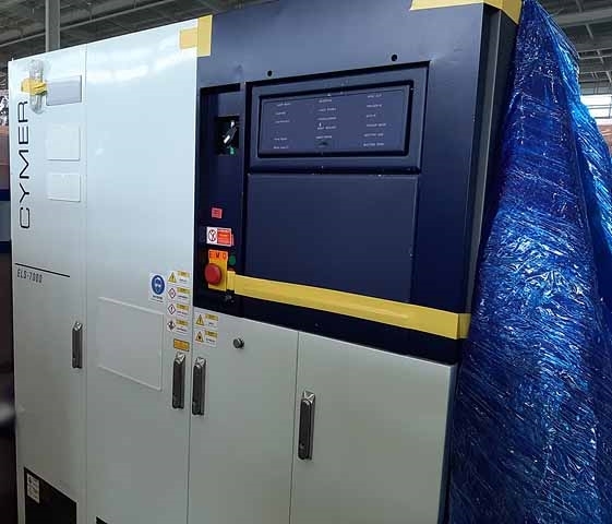

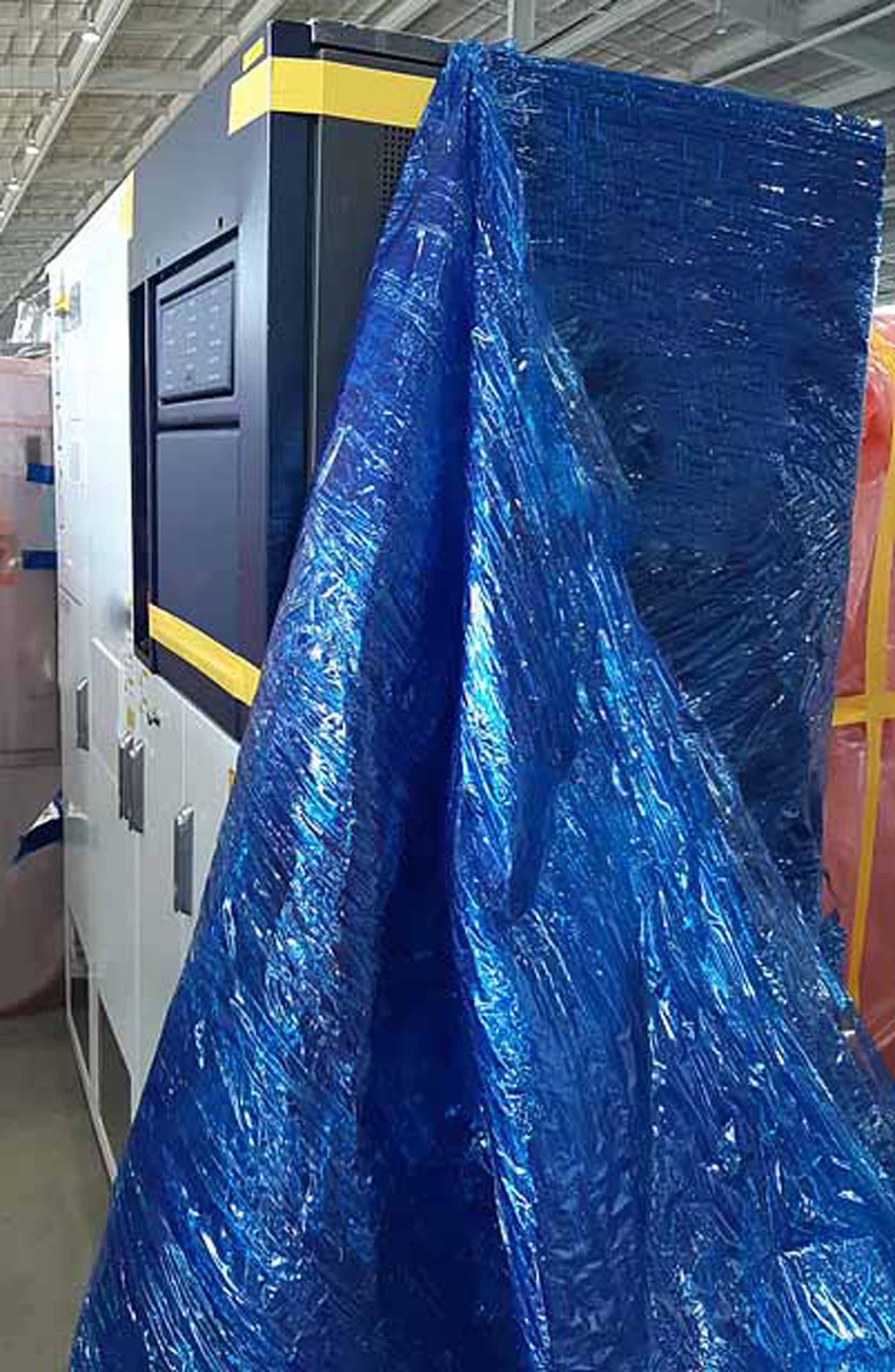

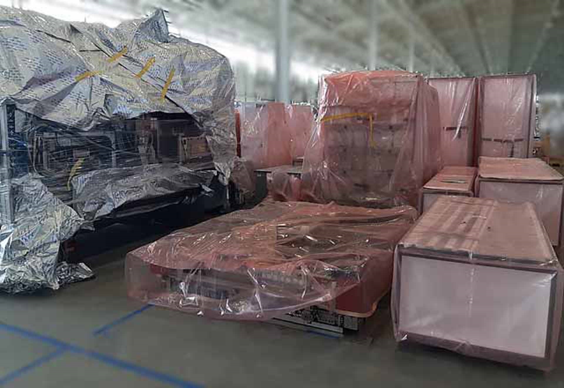

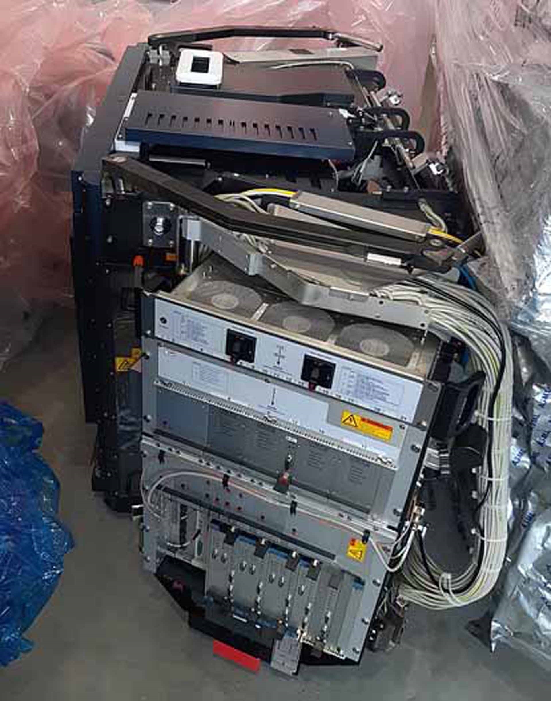

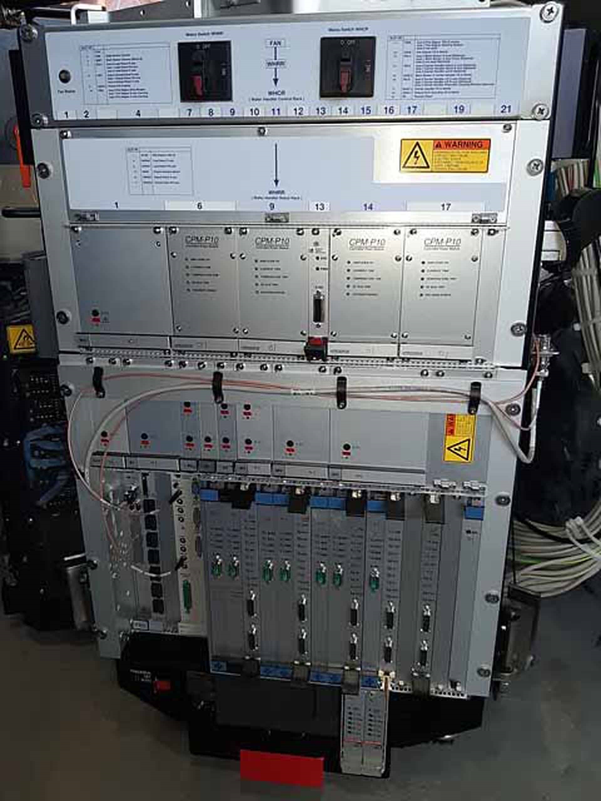

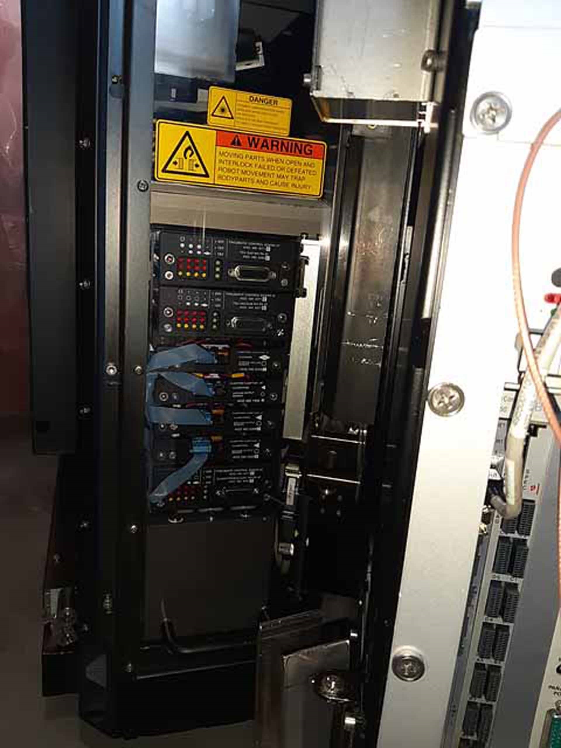

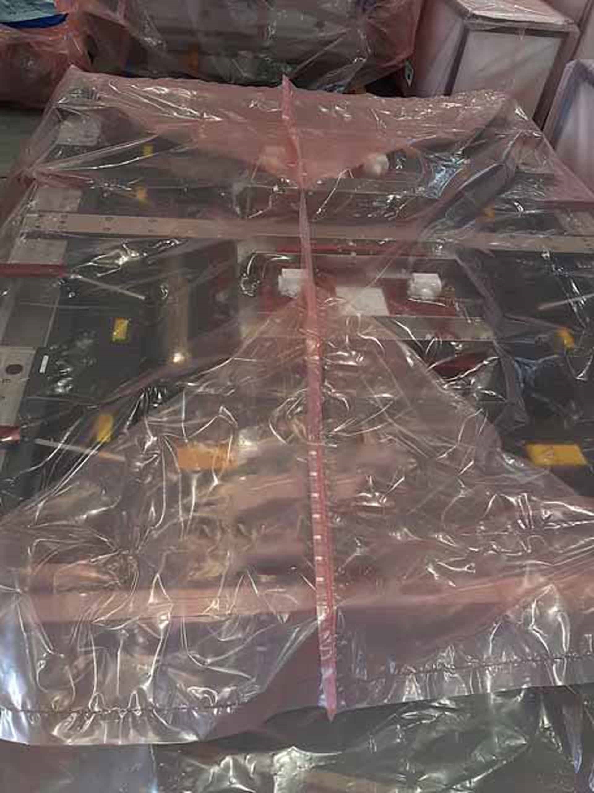

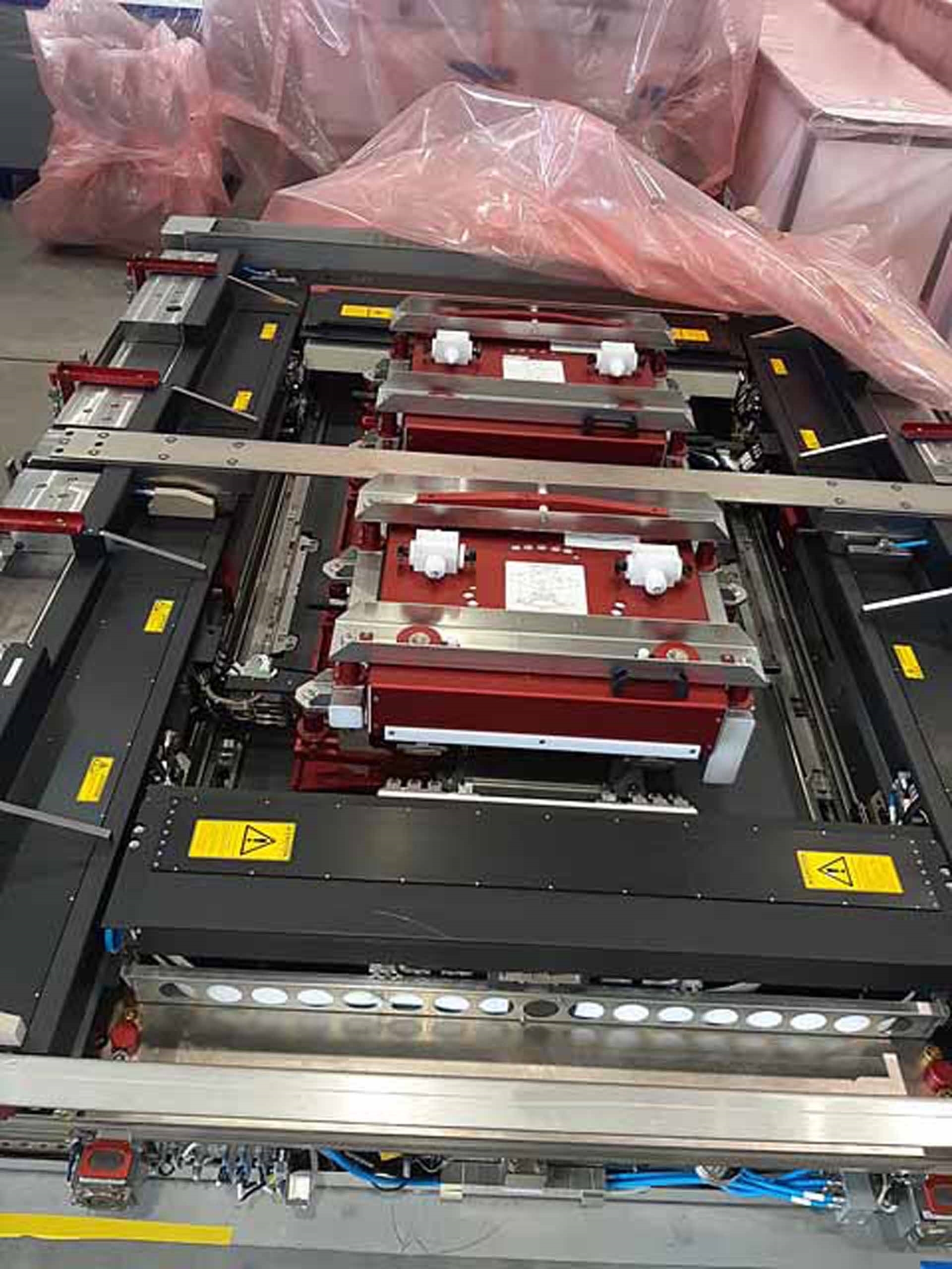


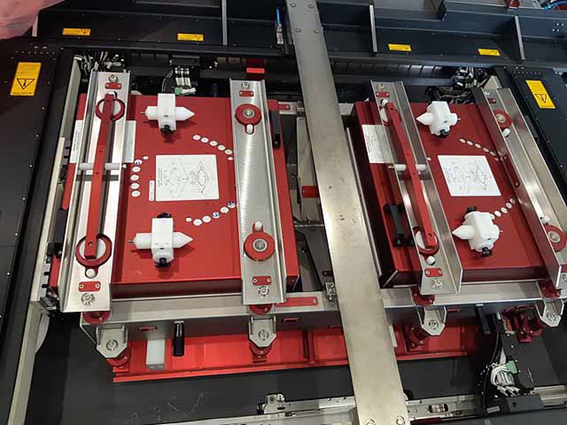

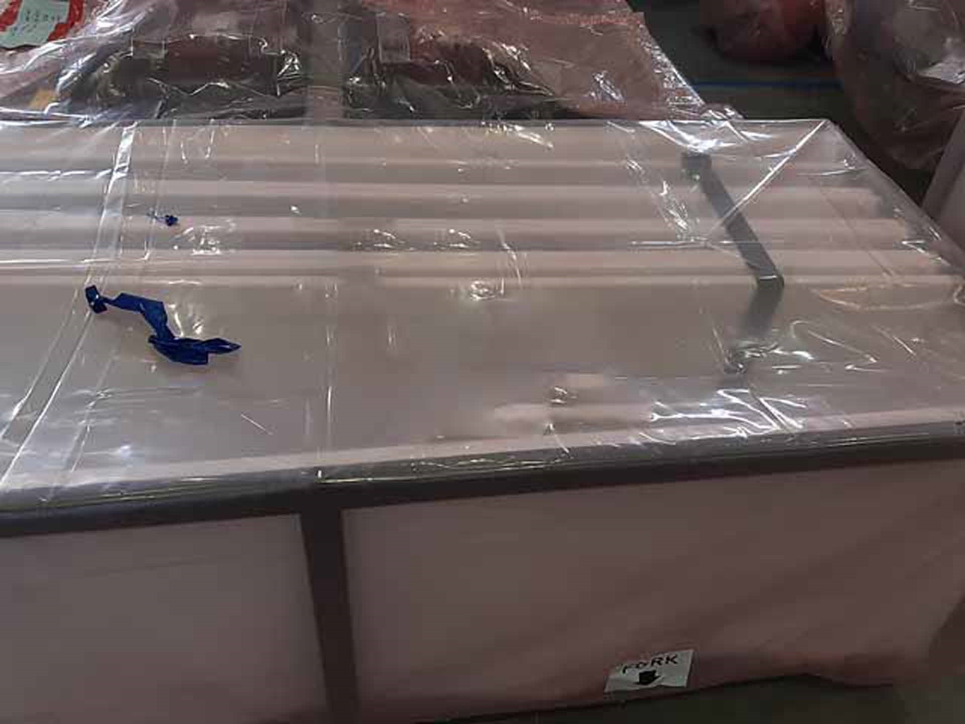

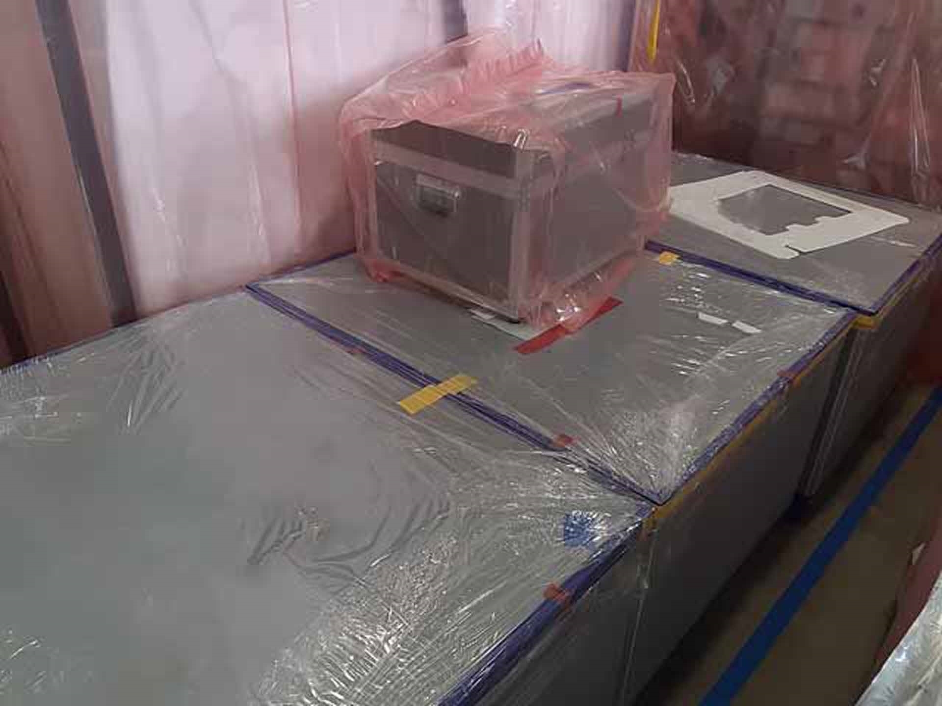

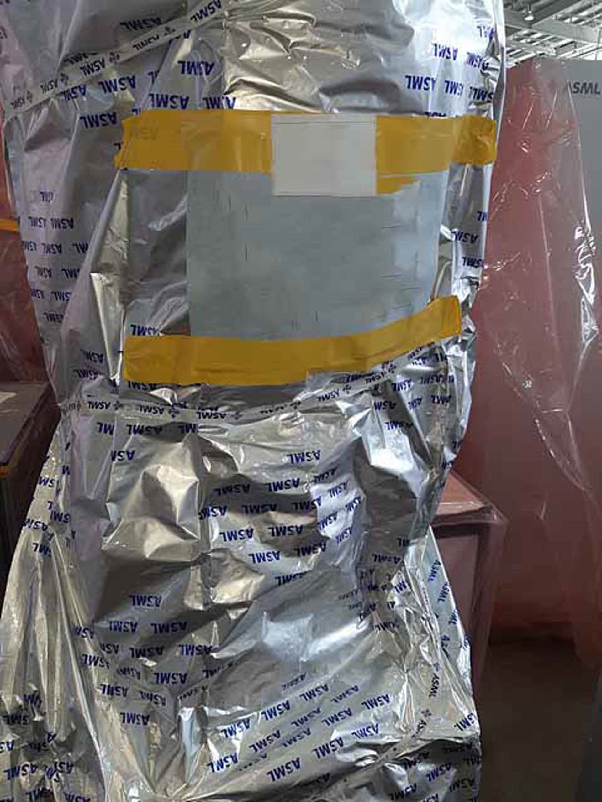

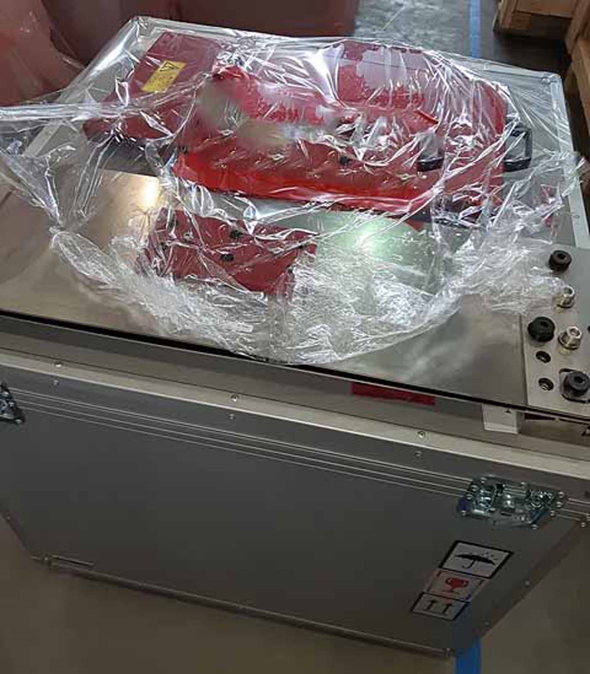


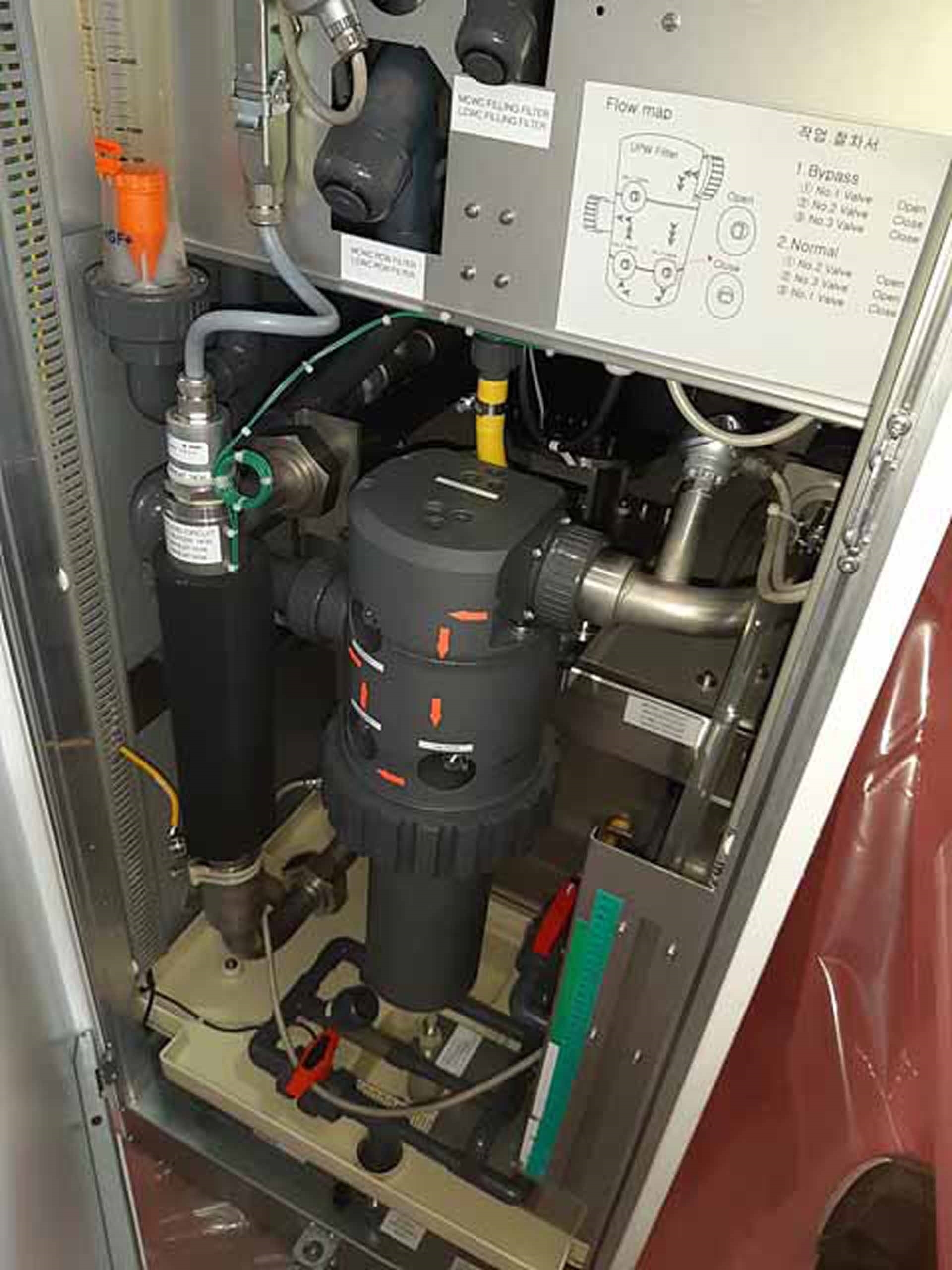

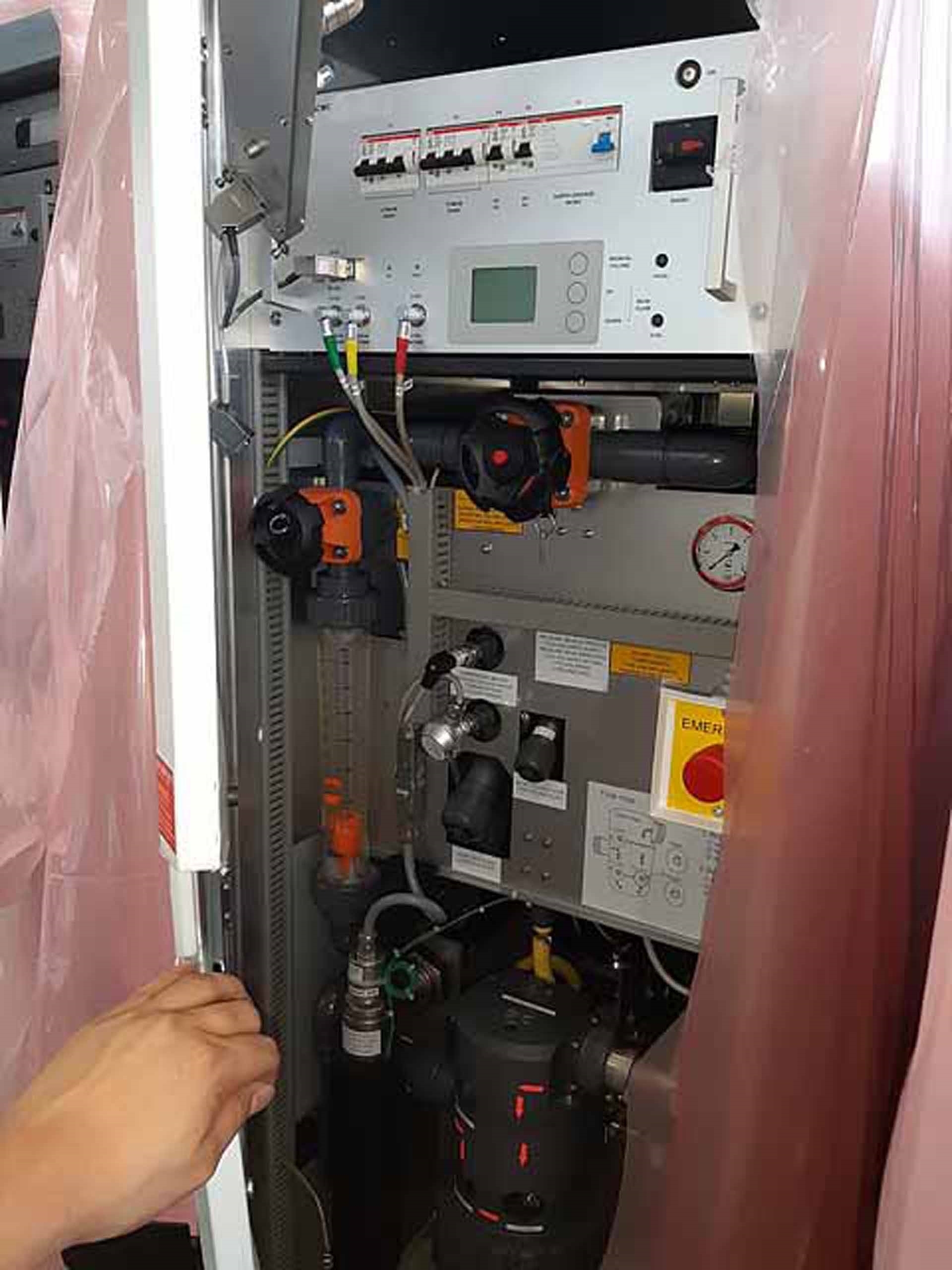

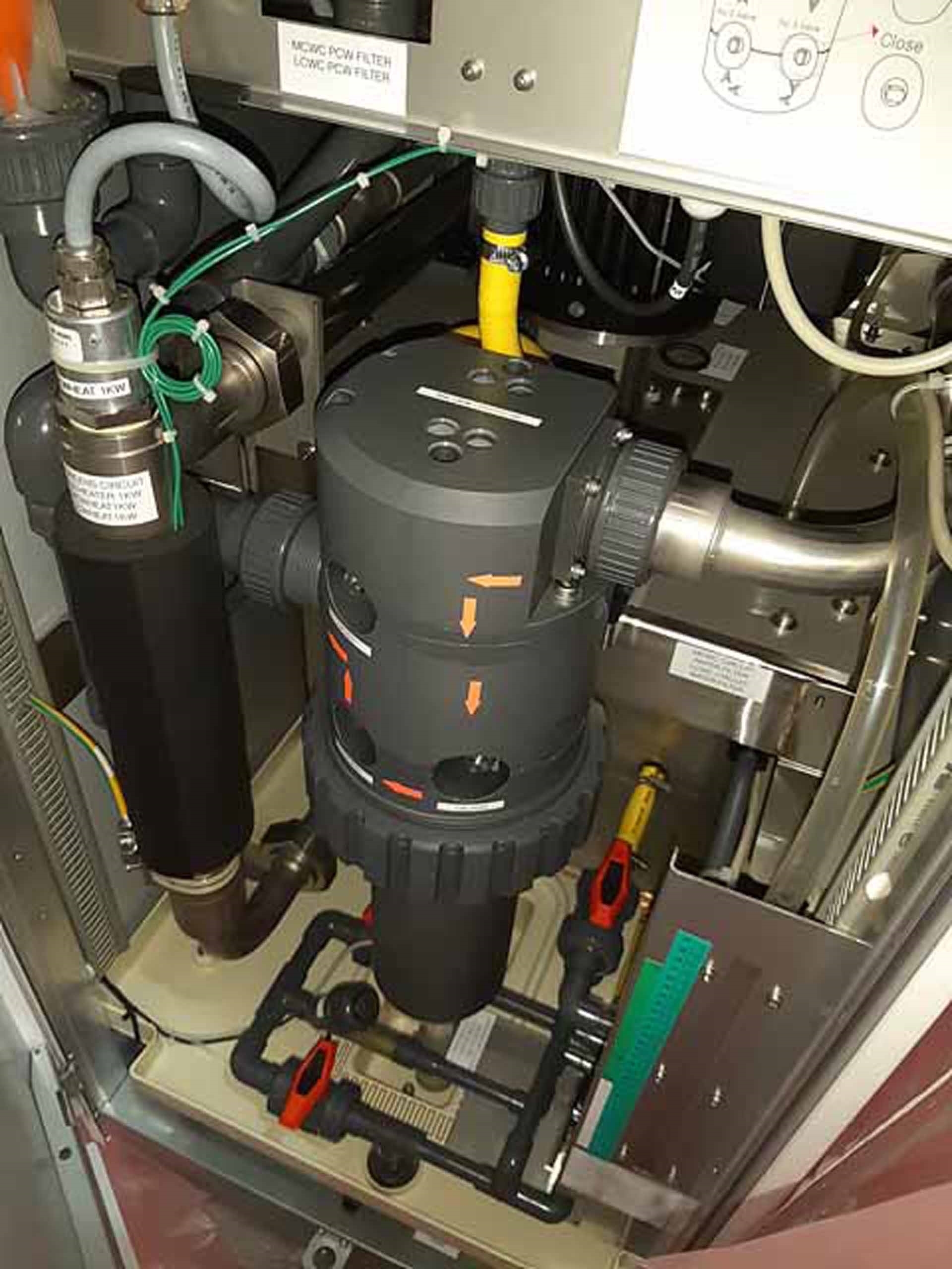


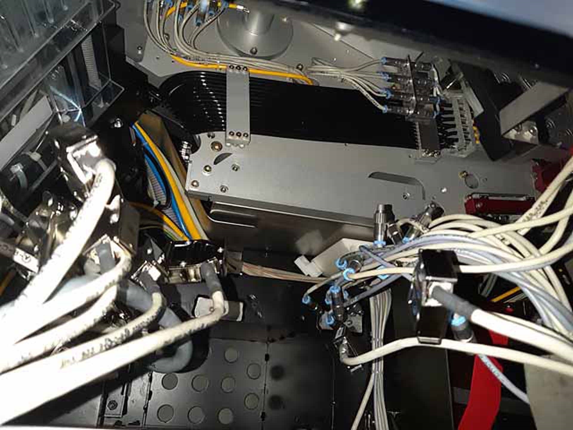

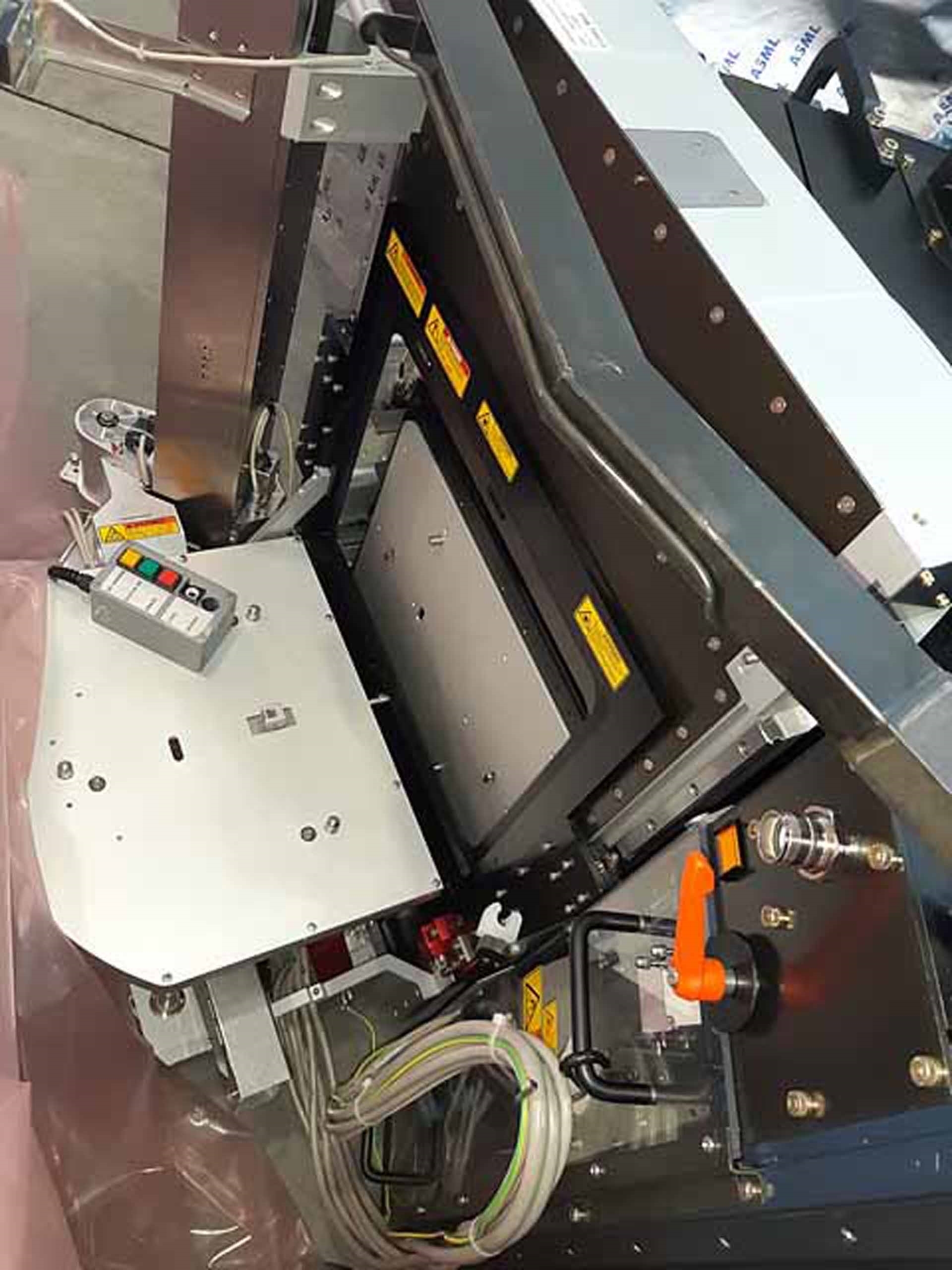


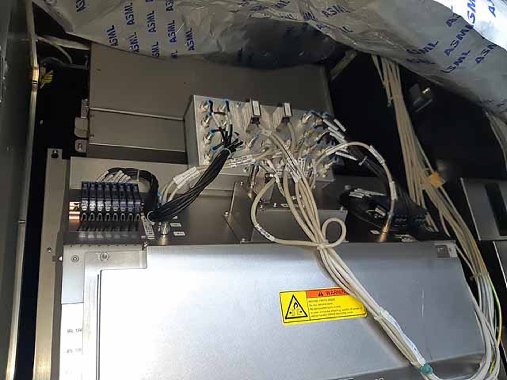


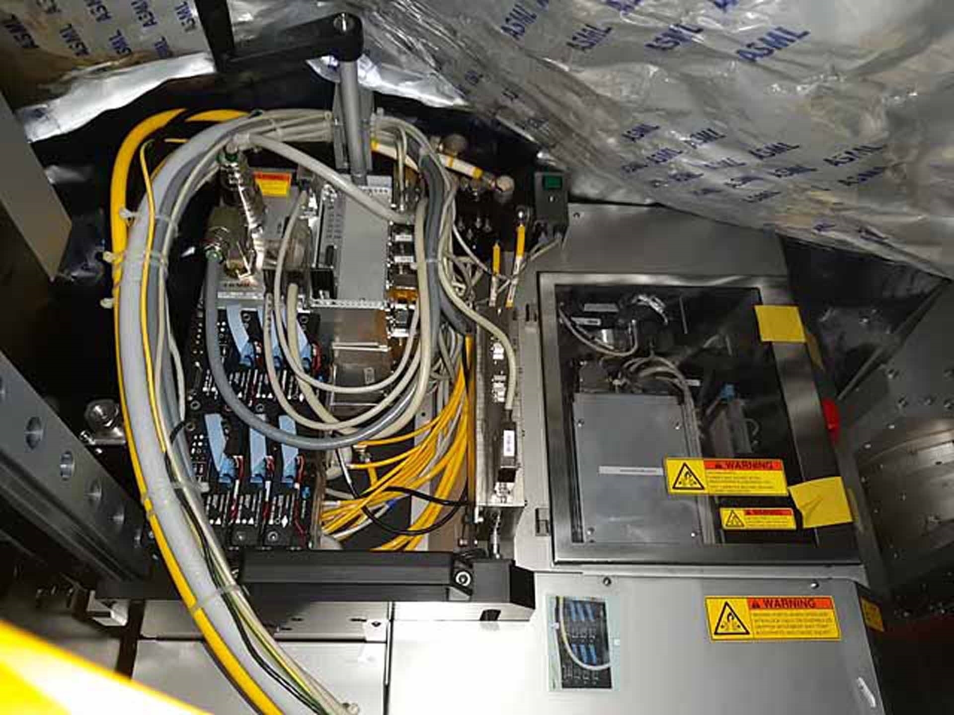

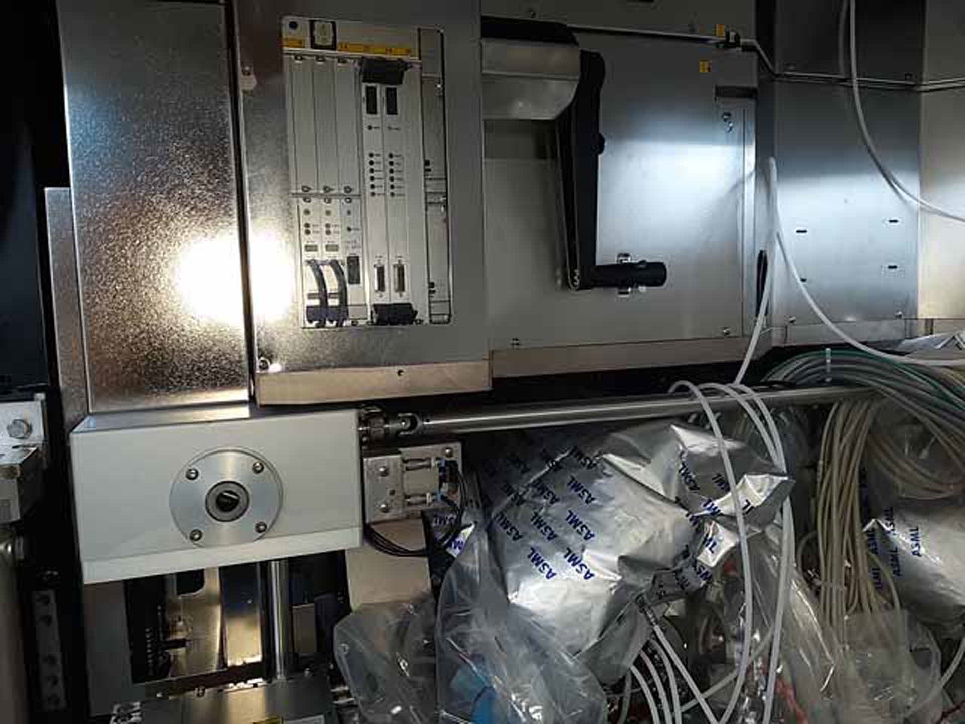

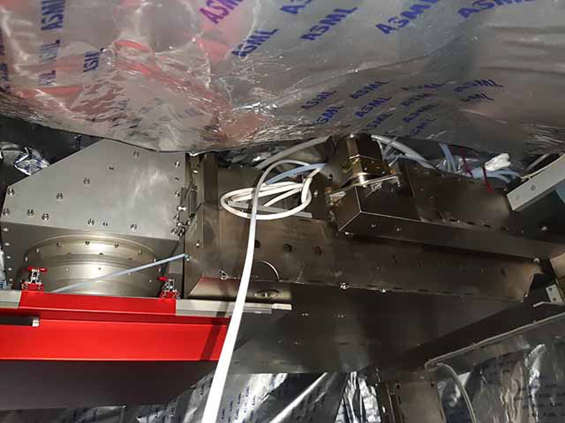

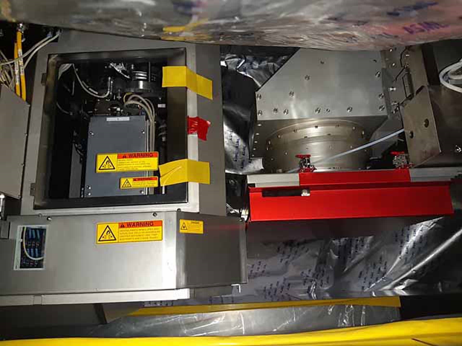

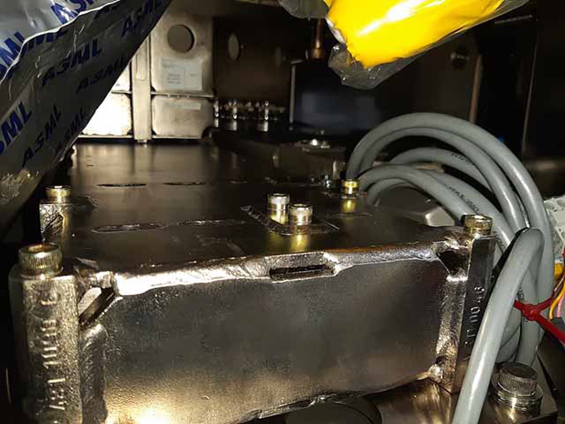

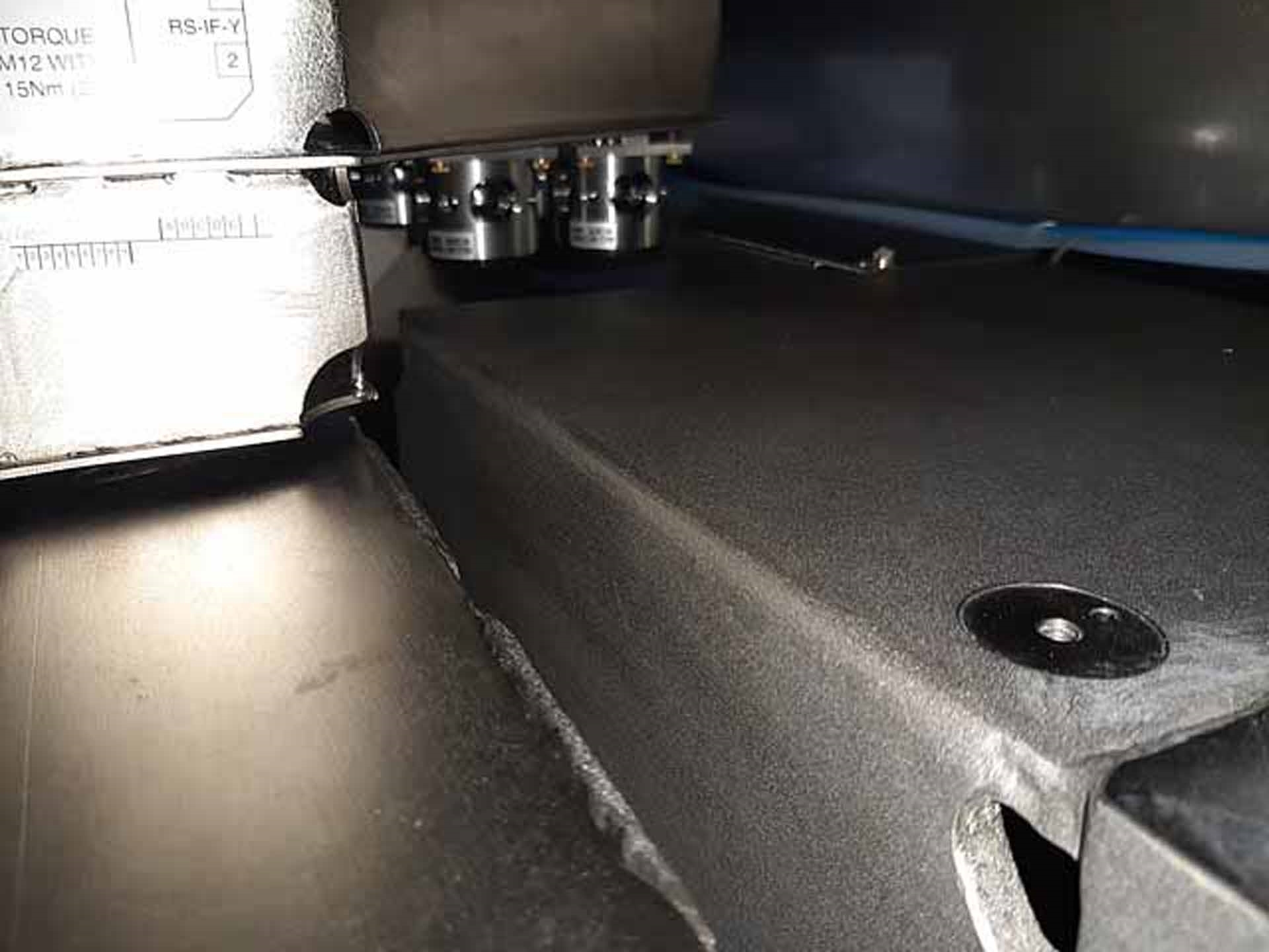


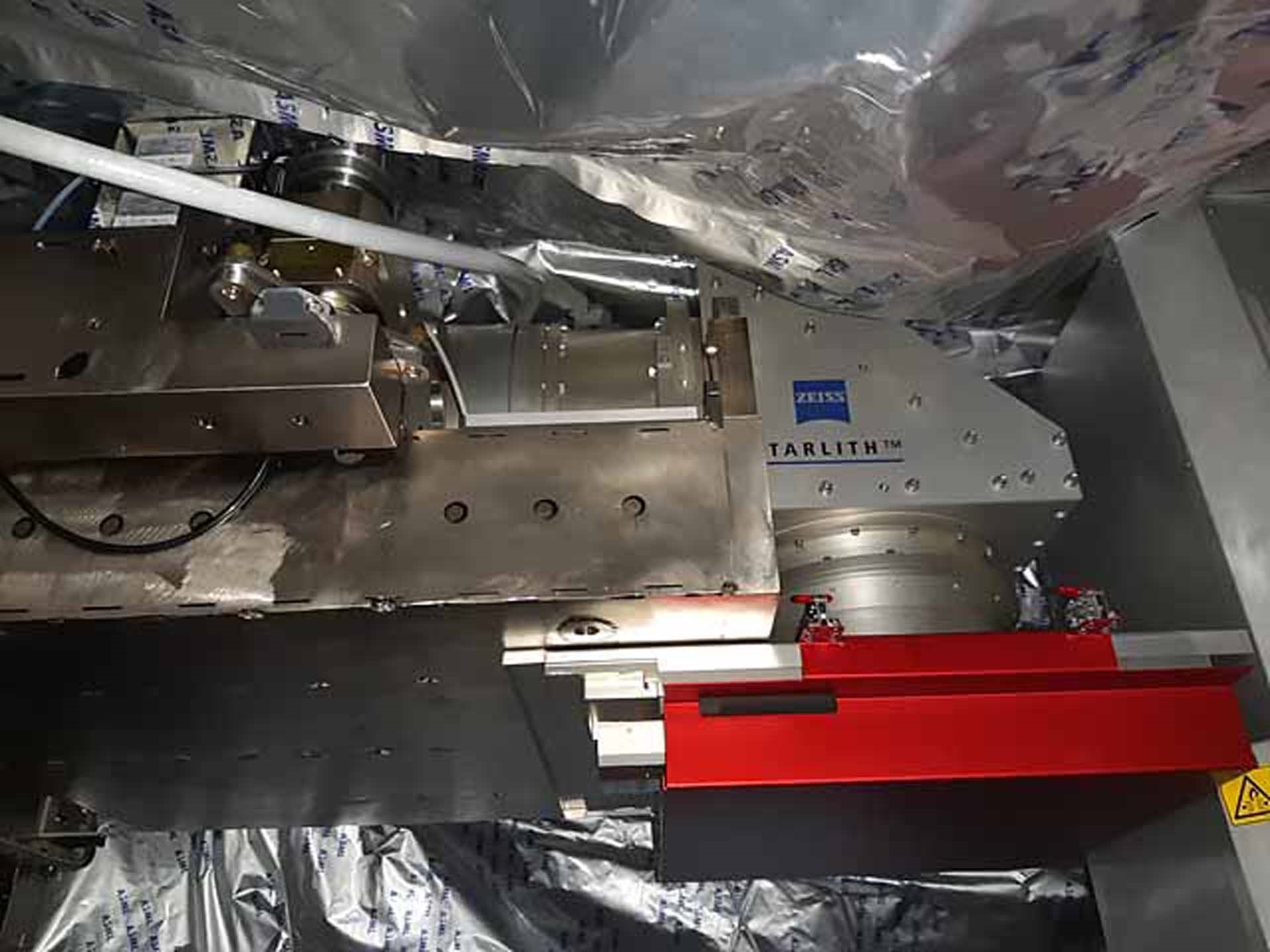

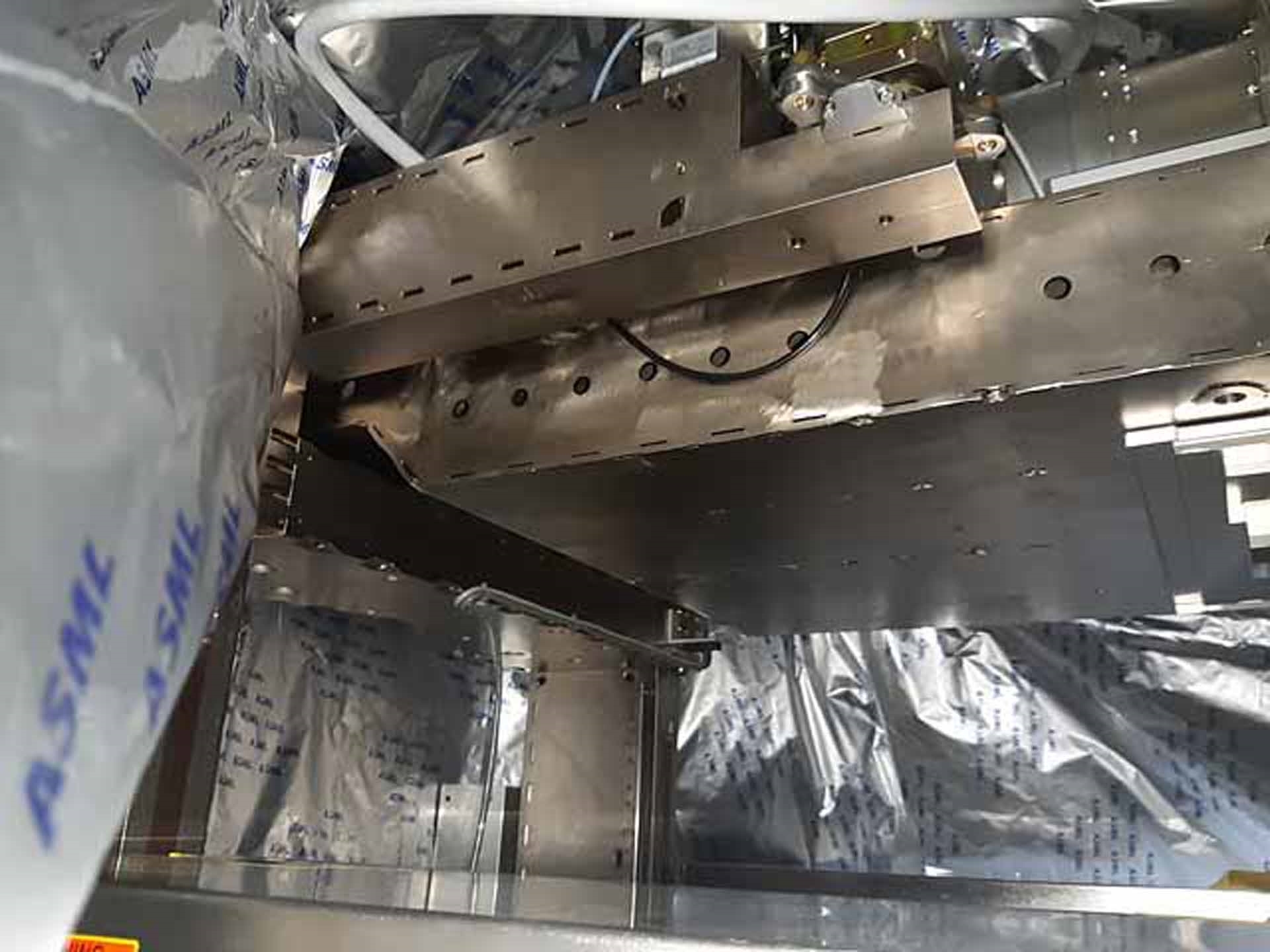

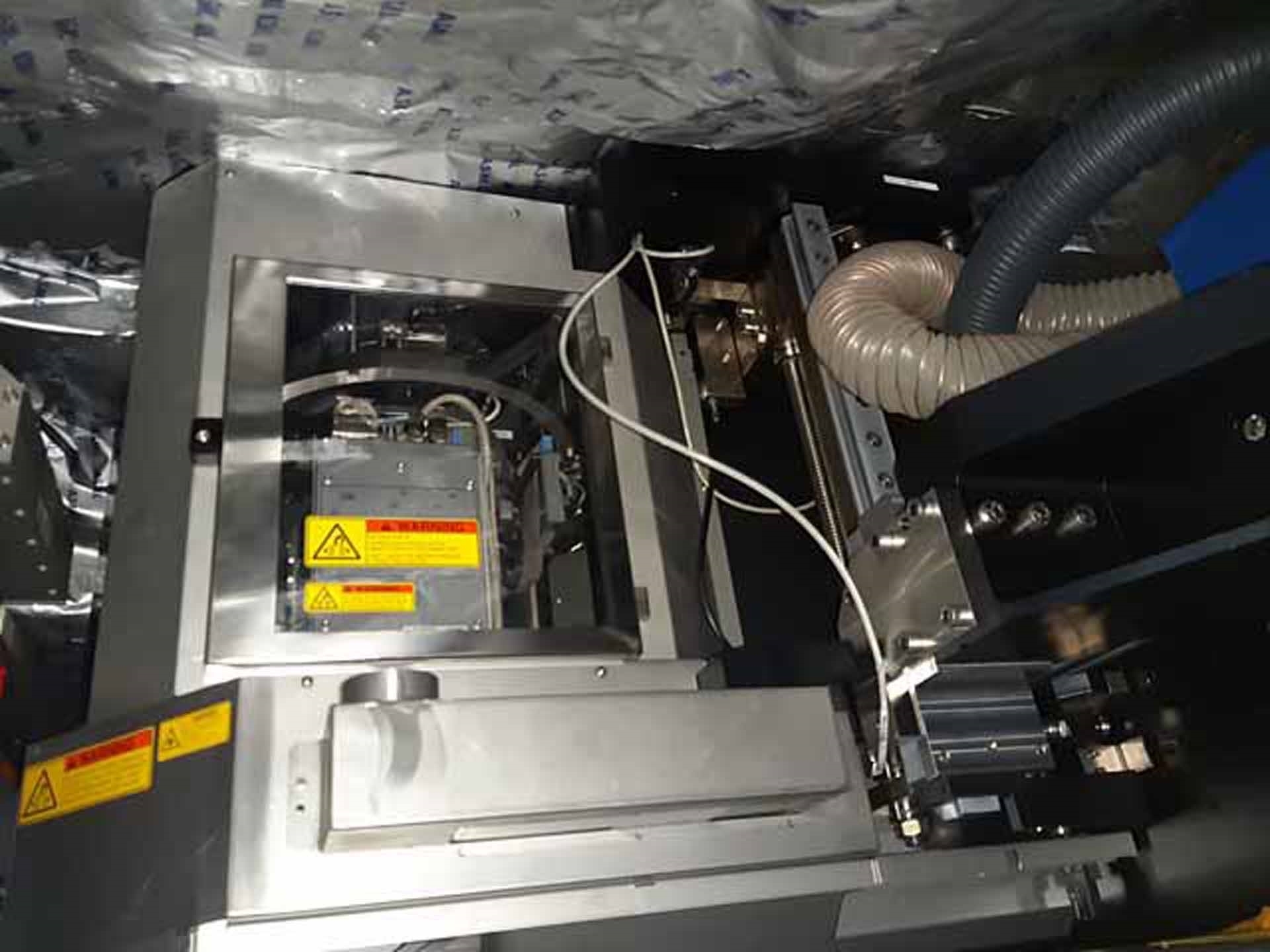


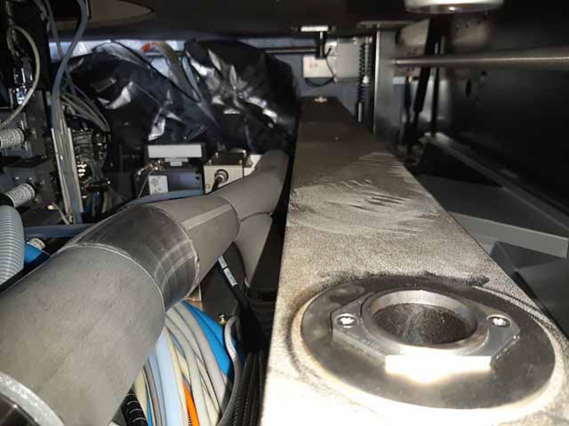

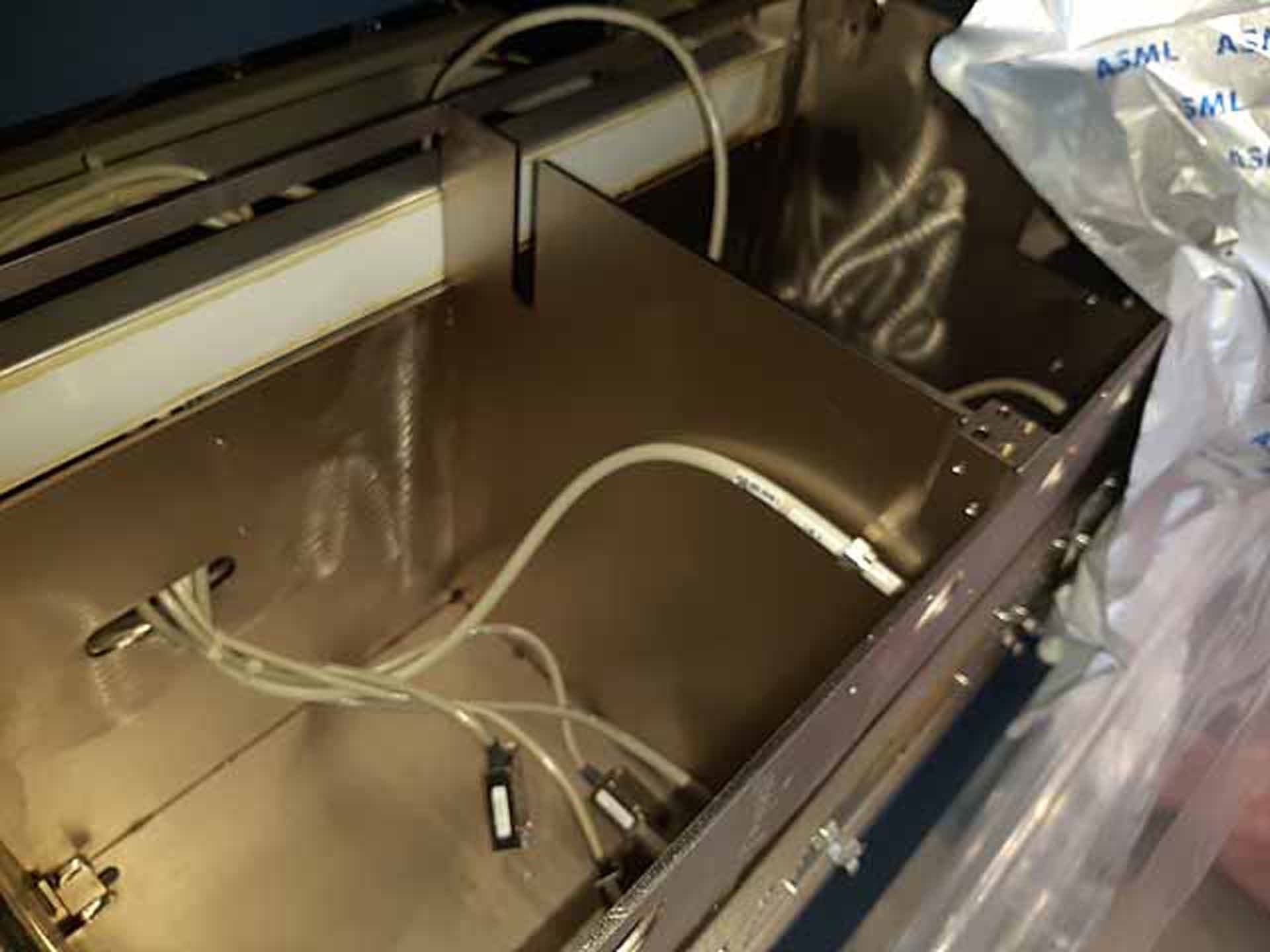

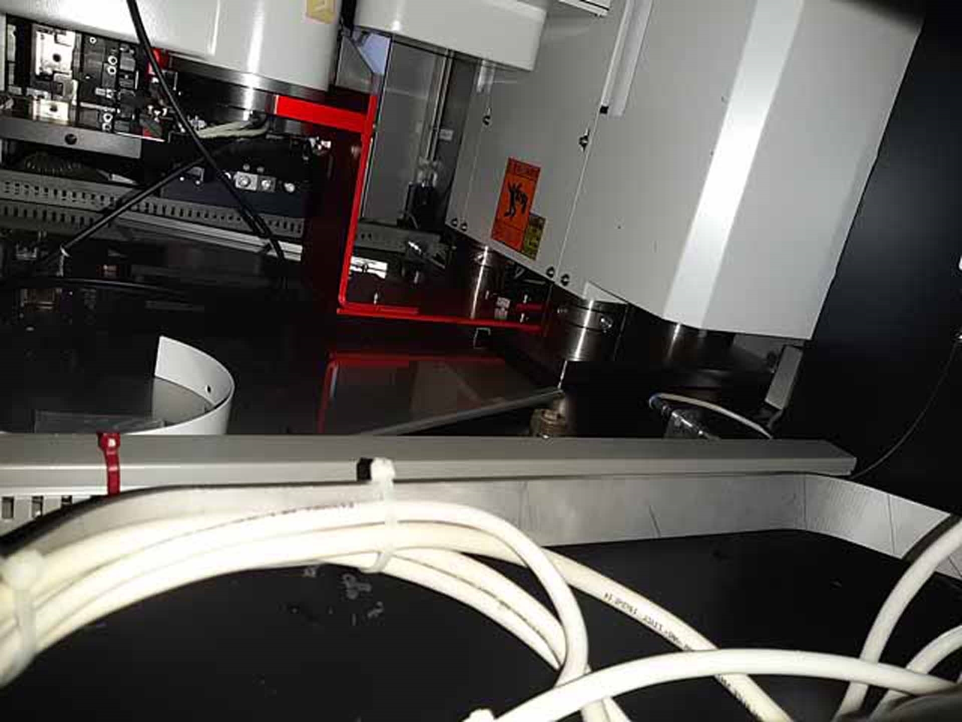




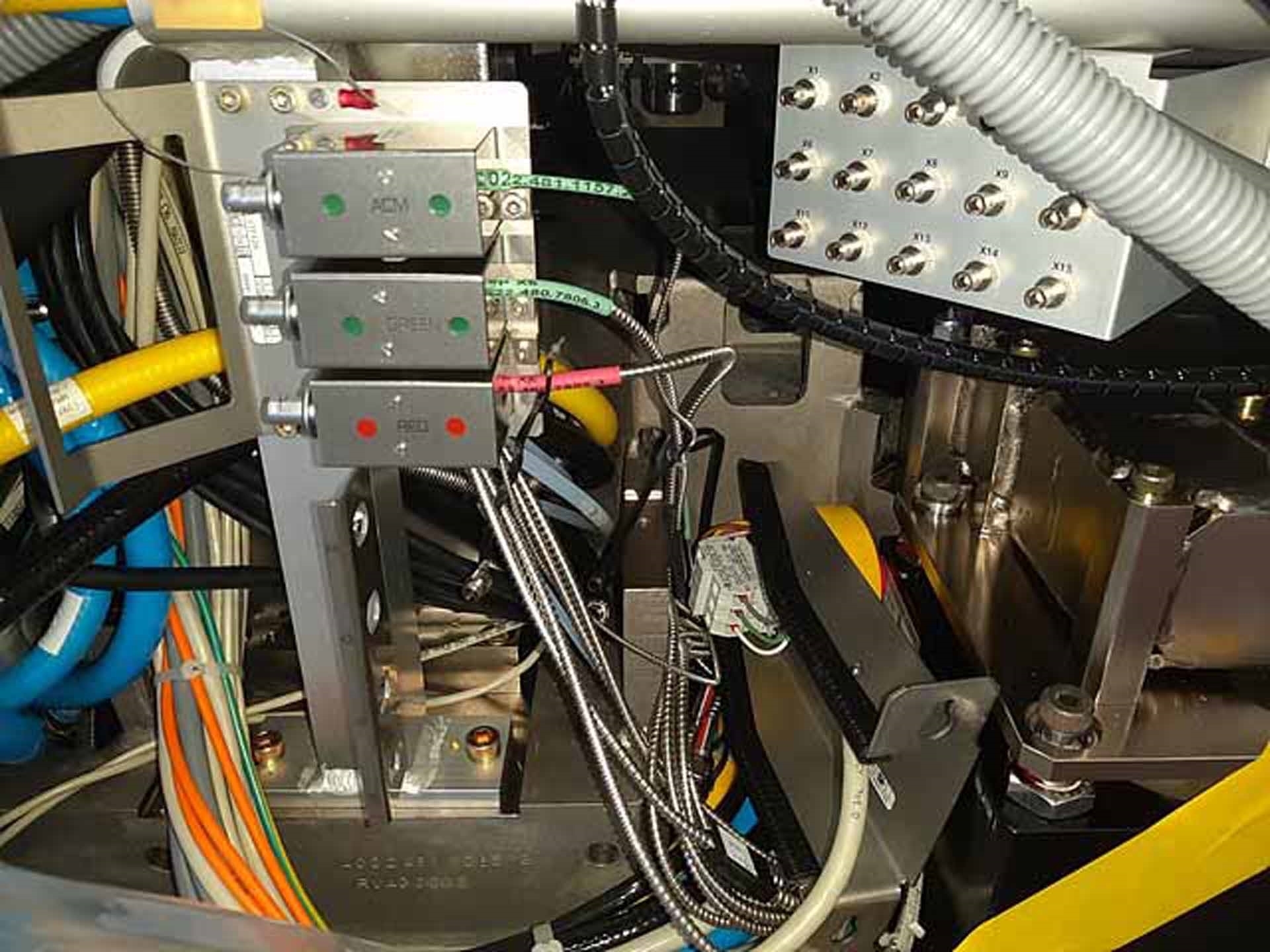

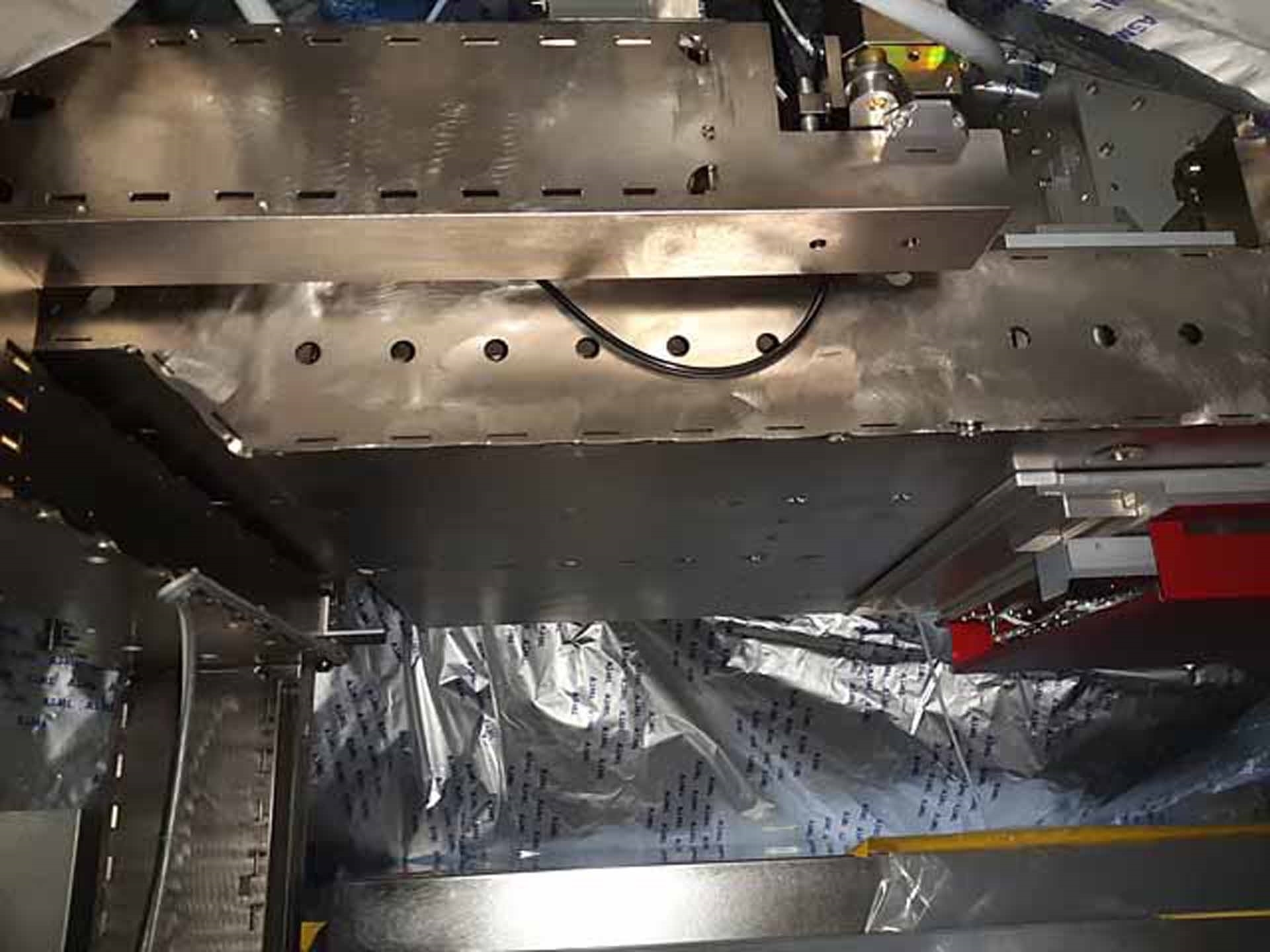


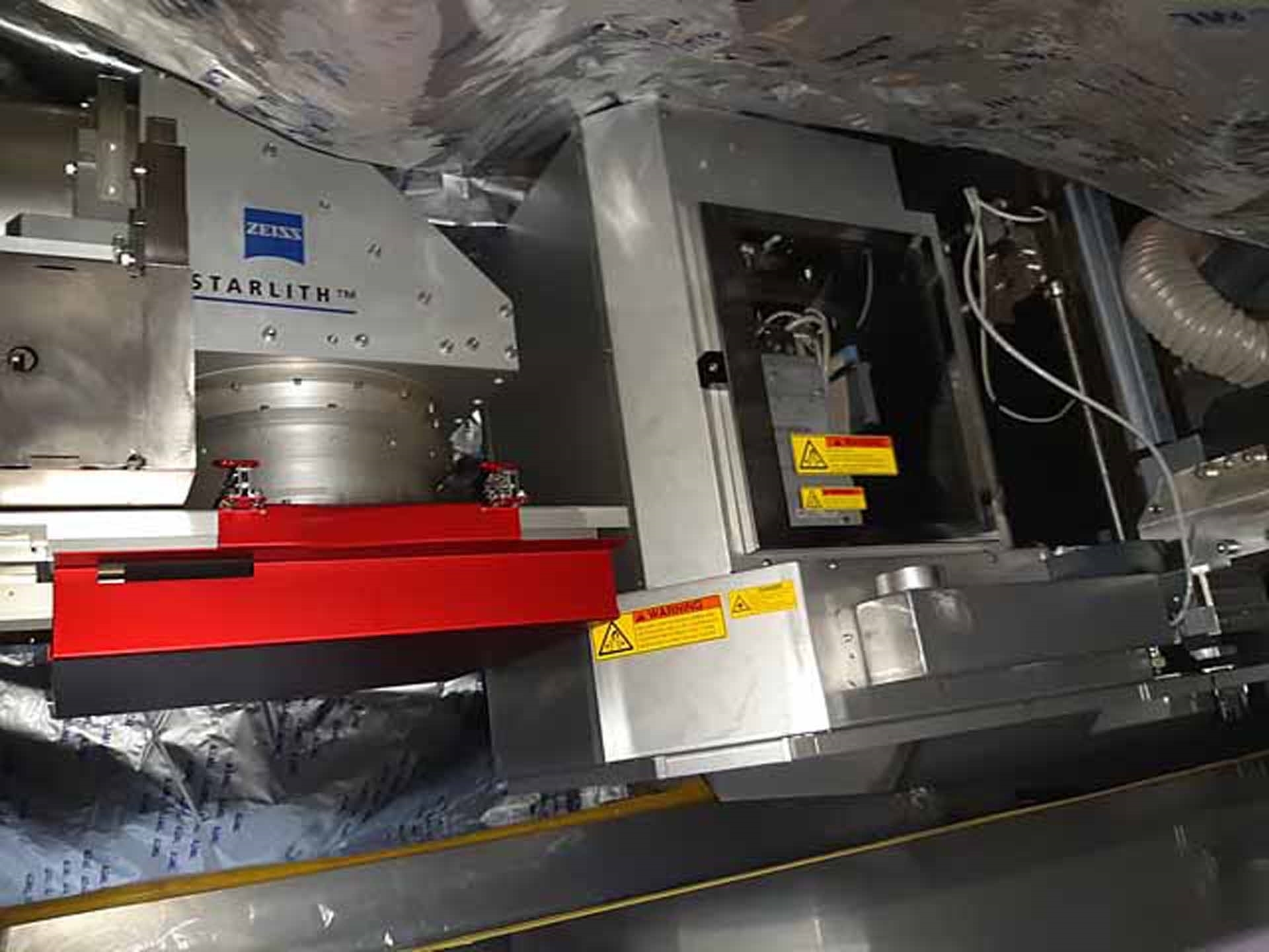


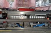
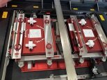
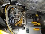
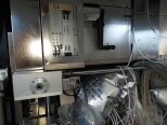
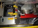
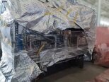
ASML AT-850C is a wafer stepper used in the semiconductor fabrication process. It is a high-throughput, high-precision optical lithography equipment designed to rapidly expose wafers to pre-defined patterns. In the chip fabrication process, ASML AT850C can be used to expose patterns as small as 5 nanometers. The system consists of two parts: a console and a point-of-exposure (POE) chamber. The console contains the pattern source (for example, a MEMS device), the light source, the optics, and associated electronics needed to control the unit. The POE chamber contains all of the movable components - the stage placing the wafer in the proper position, the motor assembly for moving the stage, and the chuck that holds the wafer. The optical components of AT:850C consist of several high-precision components, such as a collimator, a mask-aligner, a projection lens, and a scanner. The collimator directs the light onto the mask-aligner which holds the pattern in place. The projection lens then magnifies the pattern before it is projected onto the wafer. The scanner is used to move the wafer to the appropriate position to capture the pattern. ASML AT 850 C also features several advanced features for improved accuracy and throughput. It utilizes a dual-head crystal scanning machine for higher resolution and faster scanning speeds. The tool also features an alignment asset that uses a laser measuring model to accurately position the reticle and the wafer relative to each other. ASML AT:850C also includes a number of other features to ensure precision and reliability, including an auto-focus capability and an edge detection equipment to provide feedback to the system on wafer alignment. The unit also includes an alignment monitor to ensure accurate mask alignment. In addition, AT 850C is capable of positioning the wafer up to 1 micron accurately and can process wafers up to 400mm in diameter with little or no distortion. The machine is capable of extremely accurate exposures for small geometries and can achieve resolutions of less than 1 nanometer. In conclusion, ASML AT 850C is a high-precision, high-throughput wafer stepper suited to the demands of the semiconductor fabrication process. Its advanced features ensure precise, repeatable exposures in a wide range of geometries and resolutions. The tool's dual-head crystal scanning asset, alignment model, and auto-focus capabilities provide reliable, accurate exposures consistently.
There are no reviews yet


