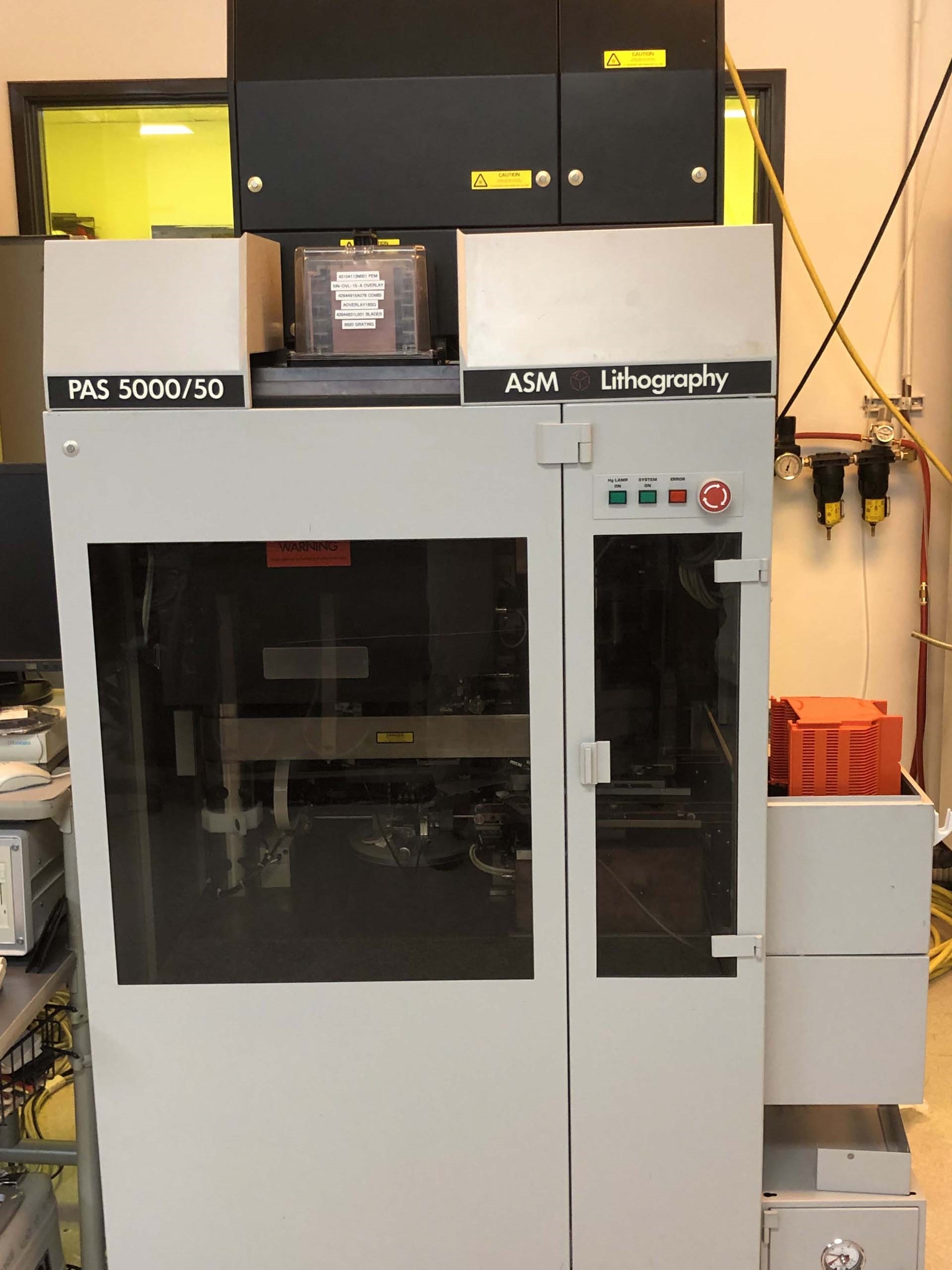
Used ASML PAS 5000 / 50 #9241835 for sale
It looks like this item has already been sold. Check similar products below or contact us and our experienced team will find it for you.
Tap to zoom


Sold
ID: 9241835
Wafer Size: 6"
Stepper, 6"
Illumination homogeneity:
15.0 x 15.0 mm (%): ≤ 3.0
9.4 x 19.0 mm (%): ≤ 3.0
Illumination intensity (mW/cm²): ≥ 245
Reticle masking (μm): ≤ 500
Lens distortion:
Non-correctable error (nm):
X 15 x 15: ≤ 120 nm
Y 15 x 15: ≤ 120 nm
Mag: <50 nm/cm
Die rotation: < 5 urad
Trapezoidal X: <50 nm/cm²
Trapezoidal Y: <50 nm/cm²
Pre-alignment accuracy (Optical sensor):
X m1 w1 (um): ≤ 7
Y m1 w1 (um): ≤ 7
Y m1 w2 (um): ≤ 7
Stage repeatability:
X [nm]: ≤ 100
Y [nm]: ≤ 100
Single machine overlay (99.7%)
X Max 99.7%: ≤ 150
Y Max 99.7%: ≤ 150
Wafer throughput:
Wafer throughput at 200 mJ/cm²: ≥ 47
Reticle exchange time (seconds): ≤ 40
UDOF: >1.2 um
Intra filed CD: ± 0.05 um @ 0.5 ± 0.025 um mean CD
Target CD reproducibility: 0.5 ± 0.05 um
Overlay:
Box in box: <150 nm
Overlay on product wafer: <150 nm
System stability:
Contamination
(3) Topside particles: 0.5um / Larger.
ASML PAS 5000 / 50 Wafer Stepper is a leading-edge tool used in semiconductor manufacturing. It prints high-resolution devices and components onto wafers in a high-throughput production environment. Specifically, ASML PAS 5000/50 is a highly accurate, deep-UV capable step and scan lithography tool with a large field size of 50-mm designed for large die sizes of 200-mm or 300-mm. It features advanced patterning technology, overlay control through an in-situ measurement system, and non-contact wafer elevators for a smooth and precise workflow. PAS 5000 / 50 stepper integrates multiple process technologies such as segmented illumination for better depths of focus, a dual optical system for improved imaging and overlay accuracy, and advanced lithographic techniques such as KrF excimer laser scanning optics along with kinematic mirror-based stage control systems. Additionally, the stepper is outfitted with high-accuracy vacuum control systems to accurately control the focus of the photomask onto the wafer. With a capability of producing 0.15-micron devices and components, PAS 5000/50 is highly reliable and repeatable, with next-level throughput and control. Its package customization options, along with its high-quality imaging and printing capabilities, make it an excellent choice for advanced lithography processes. Additionally, its low health maintenance requirements, robustness to varying production loads, and reduced cycle times contribute to its popularity in a wide range of semiconductor production environments. ASML PAS 5000 / 50 is a perfect choice for advanced, high-performance lithography processing. Its high levels of precision, accuracy, and throughput, along with its numerous process capabilities, make ASML PAS 5000/50 a great tool for any semiconductor production environment. Whether your process requires patterning or printing of high-resolution devices, or efficient and accurate overlay control, PAS 5000 / 50 will not disappoint.
There are no reviews yet