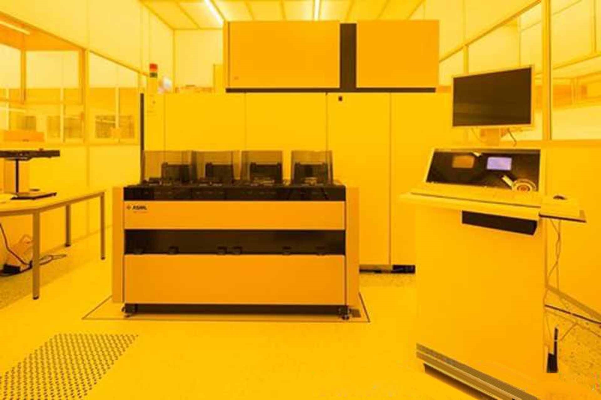
Used ASML PAS 5500 / 1100 #9219196 for sale
It looks like this item has already been sold. Check similar products below or contact us and our experienced team will find it for you.
Tap to zoom


Sold
ID: 9219196
Wafer Size: 8"
ArF Scanner, 8"
193nm Lithography
Signal tower: Local
SPM Alignmet: Standard
Optical prealign mark sensor: Standard
Wafer type: Notch
FAT Attendance
Laser type: CYMER Laser
Extended exposure
IRIS Reticles, 6"
Cassette elevator position: 1 / 2
Wafer track interface: TEL Mark 5 / 7 / 8 / ACT8
SECS I / II Interface
Batch streaming: Advanced RMS
Tape streamer OCU-MK4
Single reticle SMIF handling
Sign all
Reticle SMIF pod tag reader: Stepper version
Metrology data interface
Reticle barcode reader 24 char
Extended exposure translation
ASF E-Chuck flatness qualification
ASF Application specific lensheet
CSR CSR4066 / CSR 4442 Various
Extended exposure
Hose / Cable set: 25m
Multiple exposure
Quasar: DOE ID13 MP4 30 Included
ASF Small marks
IOSc-3 Packages
PEP 1100
Dose mapper
ASF Improved TIS measurement
Key tool performance indicators:
Focal plane deviation [nm]: 98
Astigmatism [nm]: 68
Lens distortion measured 139 points / Field:
Non-correctable error [nm]
NCE X: 2.7
NCE Y: 1.7
Dynamic performance:
Moving standard deviation mean +3 sigma: 7.5
Moving average mean +3 sigma: 1.9
Focus & levelling:
Focus repeatability (3σ) [μm]: 0.021
Level-ling repeatability:
Rx (3σ) [μrad]: 1.02
Ry (3σ) [μrad]: 1.11
Overlay performance:
Stage repeatability:
X [nm]: 1.6
Y [nm]: 3.1
Single machine overlay: 99.7% (Worst case, from stable phase) [nm]
X - Maximum 99.7%: 7.7
Y - Maximum 99.7%: 7.3
Matched machine overlay (99.7%): 10.6
Material handling:
X Position (3σ) [μm]: 0.39
Y Position (3σ) [μm]: 1.92
Rotation θ (3σ) [μrad]: 18.21
Image quality control:
3σ Image sensor measurements:
Focus repeatability: 4.78
Image tilt repeatability (Rx): 0.23
Image tilt repeatability (Ry): 0.31
Translation repeatability: 0.69
Magnification repeatability: 0.03
Die rotation repeatability: 0.06
Reticle inspection systems IRIS option:
Size and position reproduciblity: 0.997
Position range / Size standard deviation: 0.997
Inspection time [s]: 140
Stray light:
Cleaning trigger: 3.22%
Tamis:
Z7: 0.592
Z8: 1.271
Z9: 0.29
Additional elements tool include:
Laser 4kHz: Upgraded source / CYMER 7600A Laser
IRIS: Reticle inspection system
IOSc 3+: Overlay improvement
Quasar:
Automated DOE exchanger
Metrology data interface
Hertz: 60 Hertz
Power: 208 V.
ASML PAS 5500 and 1100 are wafer steppers used in the semiconductor industry for the production of integrated circuits. ASML PAS 5500 and 1100 are advanced exposure tools which employ a vertical beam of ultraviolet light to make semiconductor patterns onto photoresist on a silicon wafer. Both the PAS 5500 and 1100 are the latest scanning-projection lithography systems, utilizing a laser interferometer to achieve the best results for overlay, repeatability, and accuracy. The system offers resolution of 0.3 micrometers and numerical aperture (NA) of 0.65. A characteristic feature of the systems is their variable field size capability which enables adaptation of the beam shape for a wide variety of patterns and pitch sizes. ASML PAS 5500 and 1100 are equipped with a multi-megapixel exposure head, which helps realize sub-10 nanometer resolution. It also features improved immersion lithography, with liquid being filled between the projection lens and the wafer. This increases light transmission, leading to better image formation. The wafer stepper has an advanced servo system, which allows rapid moves and exposures of the wafer with high accuracy. It also has a number of intelligent features such as intelligent prealignment, efficient edge alignment, and efficient patterning. Additionally, the systems offer a high level of throughput and low cost of ownership. The system offers an intuitive user interface with advanced automation options, making it easy and efficient to operate. It also supports remote diagnostics and provides web-based tool monitoring systems. ASML PAS 5500 and 1100 are some of the most advanced wafer steppers in the semiconductor industry, with their high resolution and short exposure time making them ideal for fabrication of sub-micron devices.
There are no reviews yet