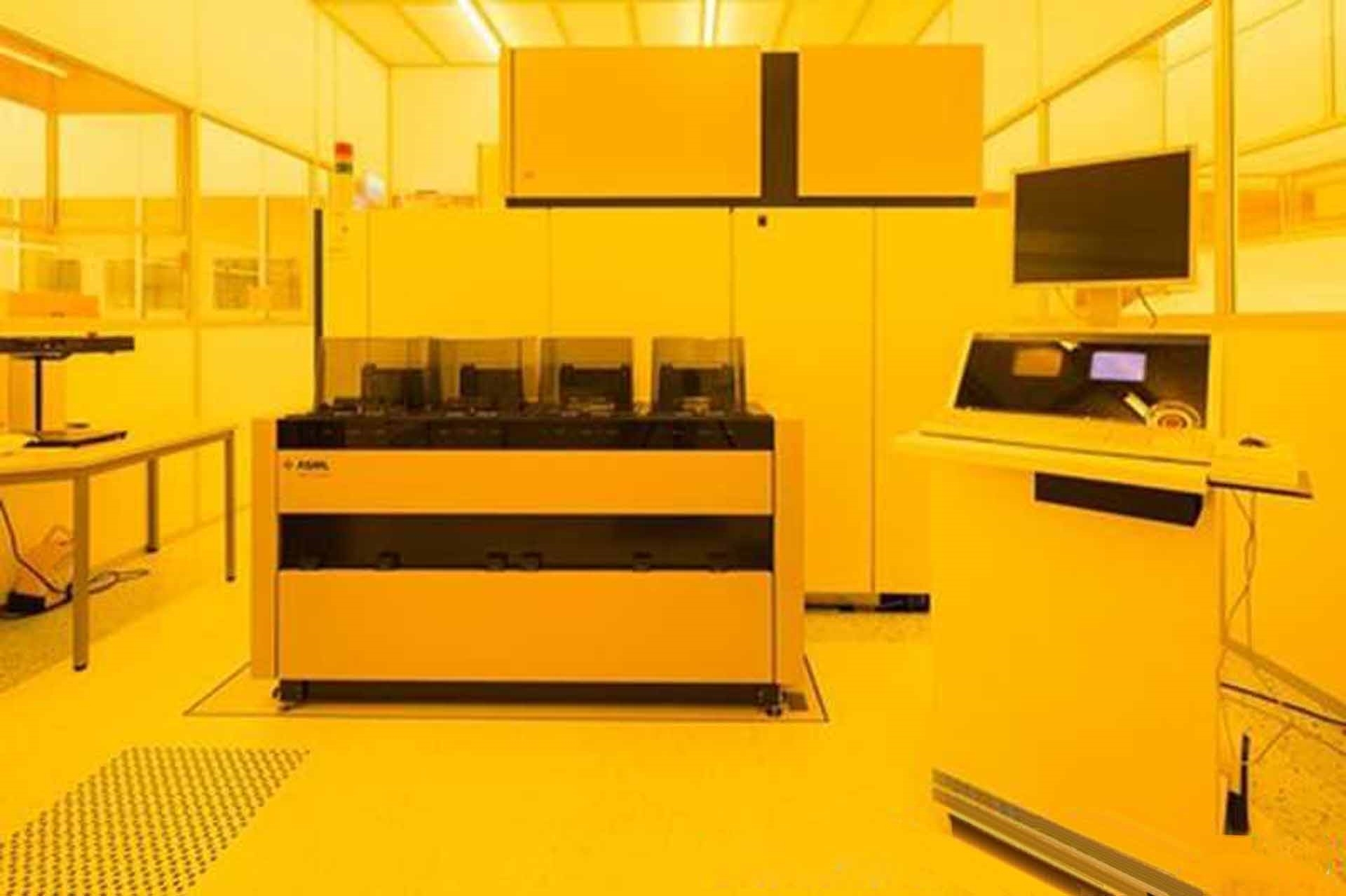
Used ASML PAS 5500 / 1100B #9161690 for sale
It looks like this item has already been sold. Check similar products below or contact us and our experienced team will find it for you.
Tap to zoom


Sold
ID: 9161690
ArF Scanner, 8"
193nm Lithography
Signal tower: Local
SPM Alignmet: Standard
Optical prealign mark sensor: Standard
Wafer type: Notch
FAT Attendance: Yes
Laser type: CYMER Laser
Extended exposure: Yes
IRIS-6 Inch reticles: Yes
Cassette elevator position: 1 / 2
Wafer track interface: TEL Mark 5 / 7 / 8 / ACT8
SECS I / II Interface: Yes
Batch streaming: Advanced RMS
Tape streamer OCU-MK4 / Less: Yes
Single reticle SMIF handling: Yes
Sign All: Yes
Reticle SMIF pod tag reader: Stepper version
Metrology data interface: Yes
Reticle barcode reader 24 char: Yes
Extended exposure translation: Yes
ASF E-Chuck flatness qualification: Yes
ASF Applic specific lensheet: Yes
CSRs Vanous: CSR4066 / CSR 4442
Extended exposure: Yes
25m Hose / Cable set: Yes
Multiple exposure: Yes
Quasar: Yes (DOE ID13 MP4 30 Included)
ASF Small marks: Yes
IOSc-3 Packages: Yes
PEP1100: Yes
Dosemapper: Yes
ASF Improved TIS measurement: Yes
Hertz: 60 Hertz
Power: 208 Volt
Key tool performance indicators:
Focal plane deviation [nm]: 98
Astigmatism [nm]: 68
Lens distortion measured 139 points / field:
Non-correctable error [nm]
NCE X: 2.7
NCE Y: 1.7
Dynamic performance:
Moving standard deviation mean +3 Sigma: 7.5
Moving average mean +3 Sigma: 1.9
Focus repeatability (3σ) [μm]: 0.021
Level-ling repeatability:
Rx (3σ) [μrad]:1.02
Ry (3σ) [μrad]:1.11
Overlay performance:
Stage repeatability:
X [nm]: 1.6
Y [nm]: 3.1
Single machine overlay: 99.7%
X - Max 99.7%: 7.7
Y - Max 99.7%: 7.3
Matched machine overlay (99.7%): 10.6
Material handling:
X Position (3σ) [μm]: 0.39
Y Position (3σ) [μm]: 1.92
Rotation θ (3σ) [μrad]: 18.21
Image quality control:
3σ Image sensor measurements:
Focus repeatability: 4.78
Image tilt repeatability (Rx): 0.23
Image tilt repeatability (Ry): 0.31
Translation repeatability: 0.69
Magnification repeatability: 0.03
Die rotation repeatability: 0.06
Reticle inspection systems IRIS option:
Size and position reproduciblity:
Position range / Size standard deviation: 0.997
Inspection time [s]: 140
Stray light:
Cleaning trigger: 3.22%
Tamis:
Z7: 0.592
Z8: 1.271
Z9: 0.29
Additional elements tool include:
Laser 4kHz: Upgraded source / CYMER 7600A Laser
IRIS: Reticle inspection system
Dose mapper
IOSc 3+: Overlay improvement
Quasar:
Automated DOE exchanger
Metrology data interface.
ASML PAS 5500 / 1100B is a wafer stepper, a type of machine used by the semiconductor industry to create integrated electronic circuits. It is used to transfer a photomask (a photographic image containing circuit patterns) onto an ultra-thin wafer. PAS 5500 / 1100B is a high-performance device that supports a wide range of materials and device sizes. It has a two-stage scanning system that is capable of producing highly accurate structures. ASML PAS 5500 / 1100B utilizes a combination of optical lenses, scanning technology and precision-contoured tracks to accurately and consistently create sub-micron feature sizes on wafers. It also uses an innovative illuminator design which reduces the amount of distortion of the photomask image while ensuring higher resolution. This system operates at speeds of up to three hundred wafers per hour and provides high throughput capabilities. PAS 5500 / 1100B requires minimal setup time and can be easily integrated into a production line. It employs high-speed, fully automated, wafer handling. This allows it to quickly recognize, scan, and transfer the photomask to the wafer without the need for any human intervention. ASML PAS 5500 / 1100B is highly reliable and can process a wide range of wafers, from large to small. It has a small footprint and is capable of running in standard production modes, for both high-volume and low-volume production. The system also supports extremely delicate functions such as pattern printing, alignment, and micro-scanning. PAS 5500 / 1100B is one of the most widely used systems for photolithography in the semiconductor industry. It provides a reliable and precise solution for creating high-quality integrated circuits. This technology has enabled the semiconductor industry to produce higher quality, smaller, and more complex integrated circuits in a cost-effective and faster manner.
There are no reviews yet