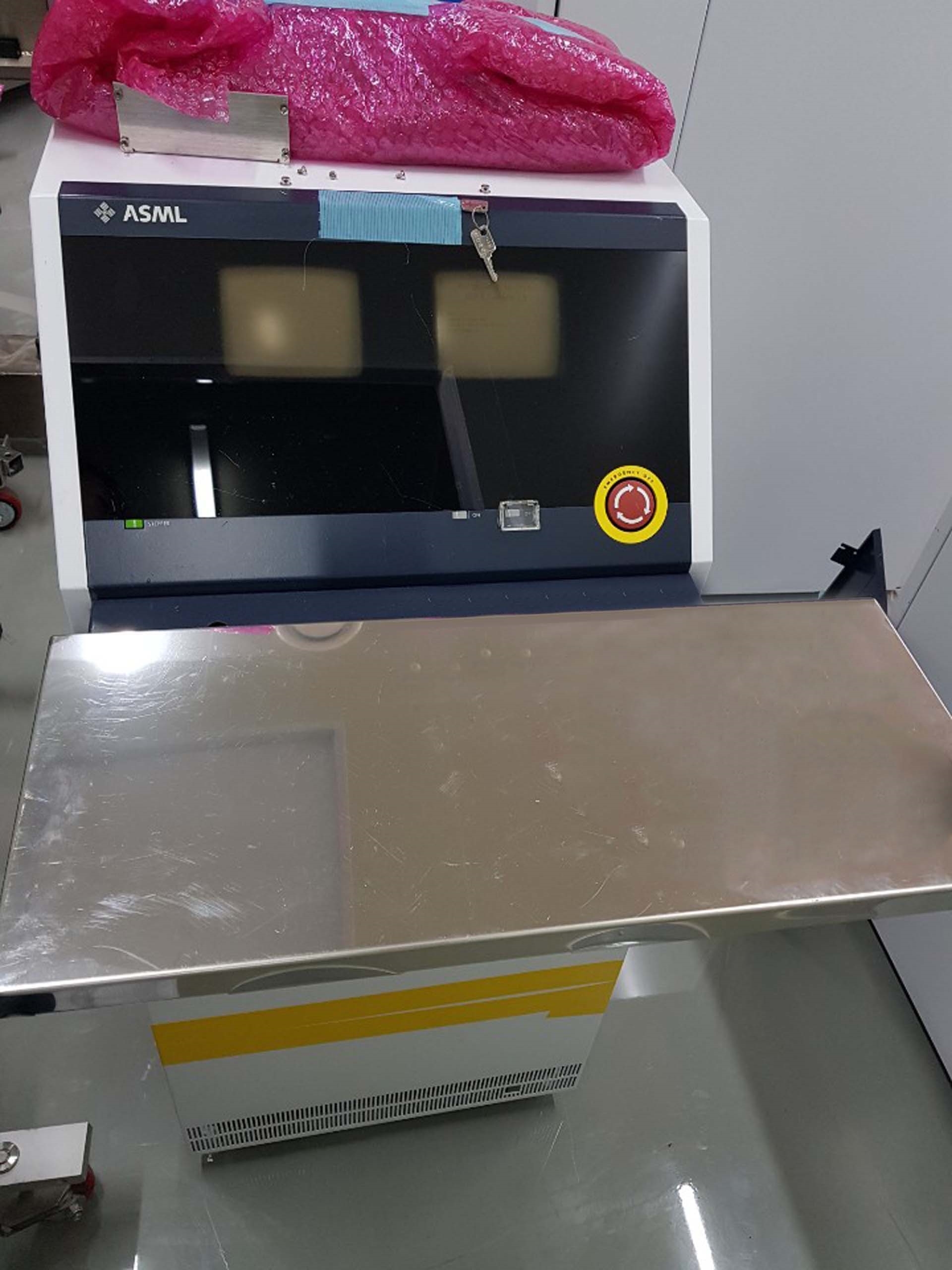
Used ASML PAS 5500 / 400D #9237241 for sale
It looks like this item has already been sold. Check similar products below or contact us and our experienced team will find it for you.
Tap to zoom


Sold
ASML PAS 5500 / 400D is a lithography equipment used to produce microelectronic devices such as integrated circuits, microstructures, and sensors. It utilizes a state-of-the-art optical projection lithography method to create these microscale devices on wafers. This machine consists of a mask and a lens system combined to a wafer stage. The lens unit enables a high resolution of patterns down to a few nanometers. The focus of the lens is in the 0.255 numerical aperture level, and is adjustable for different focal distances. This lens machine is mounted on a linear scan stage. This scan stage moves the mask and the wafer stage in an x-y direction. The maximum scan area is 400mm by 400mm with the highest scan speed of 75mm/s. The mask tool enables an accurate registration of the pattern to the wafer. It also allows a stable imaging environment over the wafer. This is achieved by mounting multiple lens systems and masks on the same stage. The pattern of the mask is divided in two parts: the image part and a reference data which is used to register the pattern to the wafer. The image part is formed by photomask patterns produced by the distributed images of customer patterns. The wafer stage enables a fast and accurate transfers of the pattern images from the mask to the wafer. This stage is made up of a chuck, a vision unit and a load lock unit. The chuck holds the wafer in place during the exposure process using a vacuum method. The vision unit has two CCD cameras for alignment to the mask and monitor the loading and unloading of the wafers. The load lock unit is equipped with a filter for clean air to transfer and remove the wafers in and out of the processing chamber. In conclusion, ASML PAS 6200/400D is a powerful wafer stepper that enables fast and accurate production of microelectronic components. Its lens asset provides a resolution down to a few nanometers, while the mask model provides an accurate registration of the pattern to the wafer. The wafer stage allows accurate and fast transfers of the pattern images from the mask to the wafer. Its state-of-the-art design makes it an ideal tool for producing microelectronic devices in large volumes.
There are no reviews yet