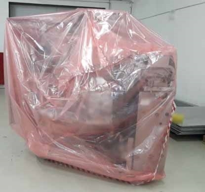
Used ASML PAS 5500 / 550D #9191419 for sale
It looks like this item has already been sold. Check similar products below or contact us and our experienced team will find it for you.
Tap to zoom


Sold
ID: 9191419
Vintage: 2000
DUV Scanner
Illumination board
Temperature cabinet: Controller
OCU: ULTRA-10 Including two hard disk
Electronics cabinet
Wafer transport system (wafer handling)
Air control cabinet
Laser & beam expander: CYMER ELS-6600 laser ( 2KHz ), 2000
ARMS:
(2) Grippers
IRIS: No
Reticle stage: Inside box
ACC Cabinet: Charcoal filter
Exposure unit check :
Visual check bottom lens
Top lens
No cystalization
Integrated slit uniformity:
(11) Scans in 26mm
Setting 1: 0.78
Illumination intensity:
(11) Scans in 26mm
Setting 1: 886
Dose repeatability and accuracy:
Dose repeatability: 0.3
Dose accuracy: 0.52
Image plane deviation: 178
Astigmatism: 76
Image distortion:
Non-correctable error: 11.5 / 8.8
Focus and leveling:
Focus repeatability (3 Sigma) : 0.01
Slit axis tilt repeatability (3 Sigma) : 0.37
Scan axis tilt repeatability: 0.39
Overlay performance:
Stage repeatability: 4.4 / 4.5
Single machine overlay using TTL alignment: 11.5 / 13.1
Athena alignment: X=11.5/Y=12.1
Wafer throughput:
8" Wafers: (46) Exposures
16 x 32 mm, 30 mJ/cm2
TTL [wafers/hour]: 117.8
Athena [wafers/hour]: 115.8
RBA [wafers/hour]: -
Intensity [mW/cm2]: 1240
Reticle exchange time:
Flash to flash reticle exchange time (s): 18.45
Image quality control:
3σ image sensor measurements focus repeatability [nm]: 23.37
Slit axis tilt repeatability [urad]: 5.79
Scan axis tilt repeatability [urad]: 1.17
Translation repeatability [nm]: 5.77
Magnification repeatability [ppm]: 0.29
Marker rotation repeatability [urad]: 0.26
Samos: 2.4
Straylight rema o/c (%): 1.11
2000 vintage.
ASML PAS 5500 is a wafer stepper used for the fabrication of ultra-miniaturized semiconductor devices. The equipment utilizes a scanning laser system, which illuminates the surface of a silicon wafer sequentially. Each area exposed to the laser is divided into a series of exposure areas, which are then printed onto the wafer in a maskless direct method. The PAS 5500 features a modern imaging unit, including a first-surface diffraction grating, an optical imaging machine, and a dual wavelength laser source. The tool has a laser wavelength range of 530-570 nm, with a spot size of 1μm. The wafer stage supports a maximum substrate size of 200mm along with a wafer-to-lens separation of 6-inch. The stepper also offers a high precision step and repeat positioning with a repeatability of +/- 1 um. Its high resolution allows for the creation of ultra-fine features and structures with minimum linewidths ranging from 0.1 to 1.0 micrometers and a pitch accuracy of less than 0.5 micrometers. It also boasts advanced alignment capabilities with an alignment accuracy of 30nm. The PAS 5500 has a high power light source that offers a maximum power of 10 kW at 500 nm and a maximum asset intensity of 1.3 J/cm2. The model has a maximum throughput of 600 wafers per hour and a maximum exposure area of 4 x 5 micrometers. Its advanced batch exposure capability allows for uninterrupted patterning jobs with large-field and multistage exposures. The equipment has an auto-alignment logic that performs automated pattern searching and alignment corrections in real time. It also offers an AutoFocus feature that strikes the optimal focus based on wafer topography. The PAS 5500 is a versatile wafer stepper suitable for photolithography and nanoimprinting. It provides high yield and high resolution imaging for the fabrication of ultra-miniaturized semiconductor devices. The system is an ideal choice for manufacturers that need a fast, reliable, and power-efficient stepper solution for their production needs.
There are no reviews yet