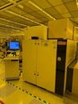
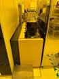
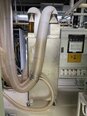
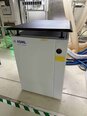
Used ASML PAS 5500 / 700B #293779167 for sale
URL successfully copied!
Tap to zoom

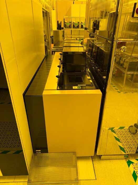
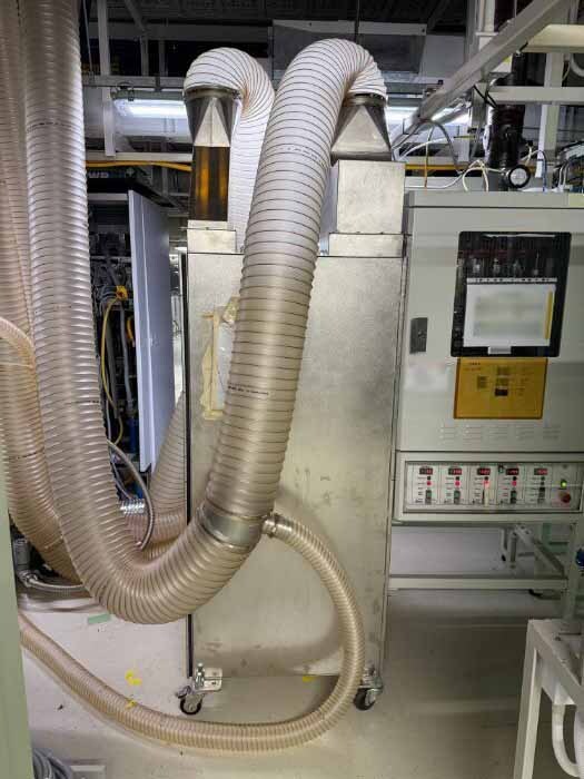
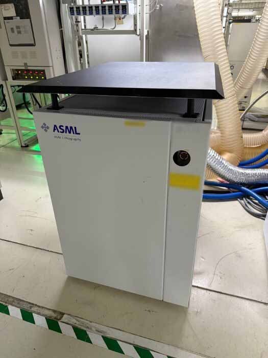
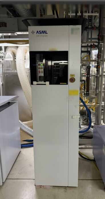
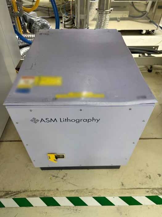
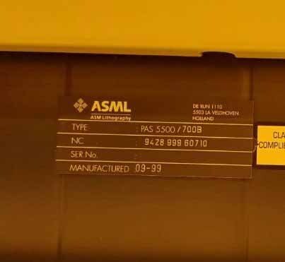
ID: 293779167
Wafer Size: 8"
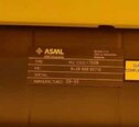
Vintage: 1999
DUV Stepper, 8"
CIM: SECS
SMIF Interface
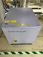
Wafer transfer unit handler system
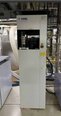
C&T Cabinet
Operator console unit
Integral slit uniformity:
Annular: ≤ 1.2
Conventional: ≤ 1.2
Illumination intensity:
Annular: 2400
Conventional: 2400
X and Y Moving standard deviation: ≤ 30 nm
X and Y Moving average: ≤ 15 nm
Dose repeatability and accuracy:
Dose repeatability: ≤ 0.7%
Dose accuracy: ≤ 2.0%
SAMOS: ≤ 5.5
Image plane deviation: ≤ 175
Astigmatism: ≤ 125
Best focus (Dynamic): 0±35 nm
Image sensor measurements:
Focus repeatability: ≤ 30 nm
(Rx) Scan axis tilt repeatability: ≤ 6.0 μrad
(Ry) Scan axis tilt repeatability: ≤ 2.0 μrad
Translation repeatability: ≤ 10 nm
Magnification repeatability: ≤ 1.0 ppm
Die rotation repeatability: ≤ 1.0 μrad
1999 vintage.
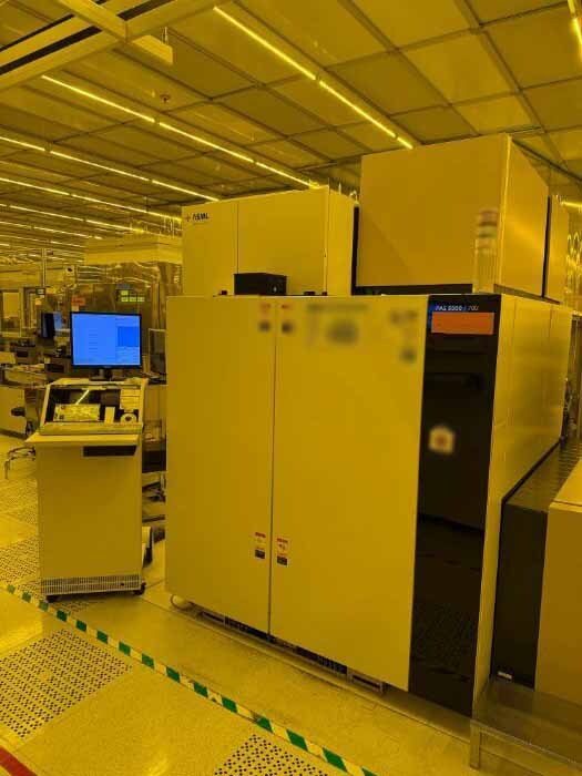
ASML PAS 5500 / 700B is a state-of-the-art wafer stepper used in photolithography. It is a scanning equipment with a commanding core that features accurate, continuous movement and long-term stability. Its main application is in the manufacture of semiconductor devices, wherein a pre-expanded wafer is transferred onto the stepper and precision alignment is achieved using lithographic exposures. The stepper is a fully automated computer-controlled imaging system. It contains a high-precision metal frame, called the wafer stage, which has both the X and Y axes of motion. The stage is motor driven and has the capability to move in 0.5- to 4.0-micron intervals. It also has the ability to measure its position with a precision of 0.1-micron size steps. Its linear encoder provides repeatable control over the movement of the stage. The wafer stage accommodates wafers up to 10" in diameter with a maximum of 45mm thick. The stepper can accommodate wafers with a thickness range within 7µm to 5mm. In addition to supporting wafers with different levels of flatness, the stepper contains a calibration unit that is capable of detecting shape errors and correcting exposed images. PAS 5500 / 700B is equipped with a high-power light source and a range of high-resolution lenses. It offers a range of exposures, including line/space and contact exposures, as well as high-aspect-ratio and complex shaped masking. Furthermore, its advanced optics setup and mirror machine allow for fine-tuning of photoresist focus and depth of field. The stepper is also equipped with a high-performance image analysis tool. It is capable of detecting defects and non-conformities in images to a level of 0.25µm. This allows for virtually perfect wafers with no defectivity. The robust, reliable, and reconfigurable design of ASML PAS 5500 / 700B allows for rapid, high-resolution stepper operation with a maximum operating speed of 35 exposures per second. Additionally, the stepper features a wide range of granularity, from full-field to partial-field exposures, providing greater flexibility in production applications. PAS 5500 / 700B is a powerful and versatile wafer stepper that provides reliable, high-resolution performances. It is a suitable tool for producing high-quality semiconductor devices. Its advanced optics, imaging asset, and automated operation allow for highly efficient and precise lithography.
There are no reviews yet