Used ASML Twinscan 850 #293799735 for sale
URL successfully copied!

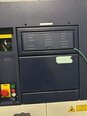
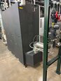
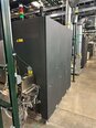
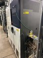
Tap to zoom
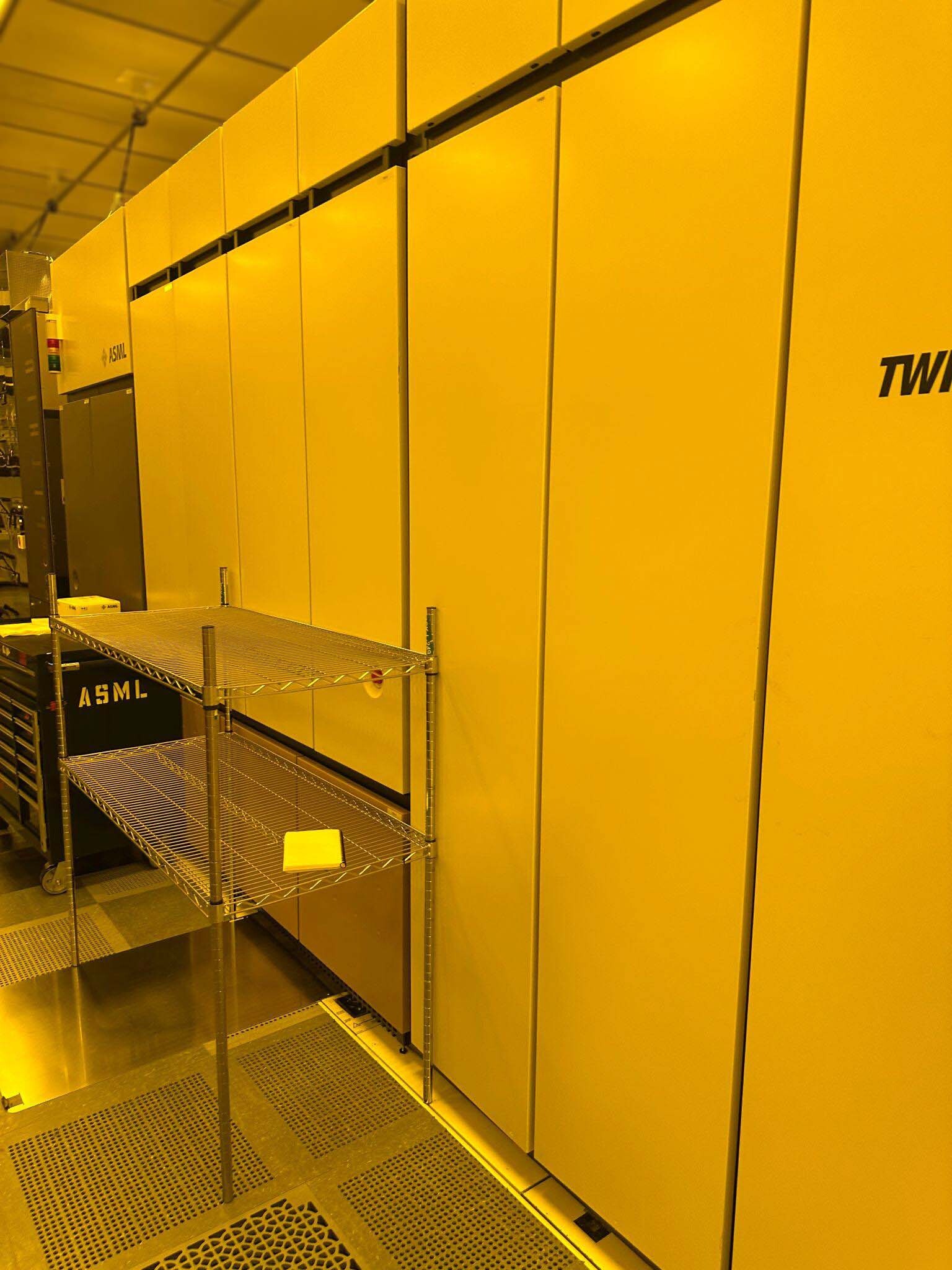

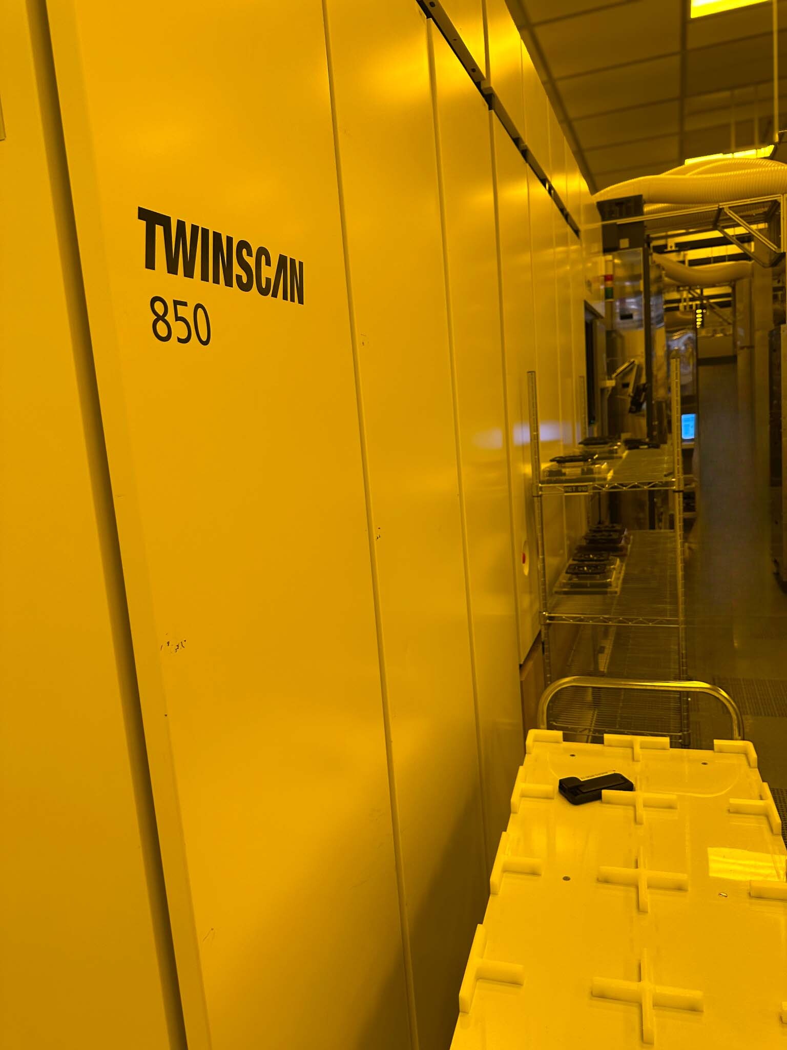
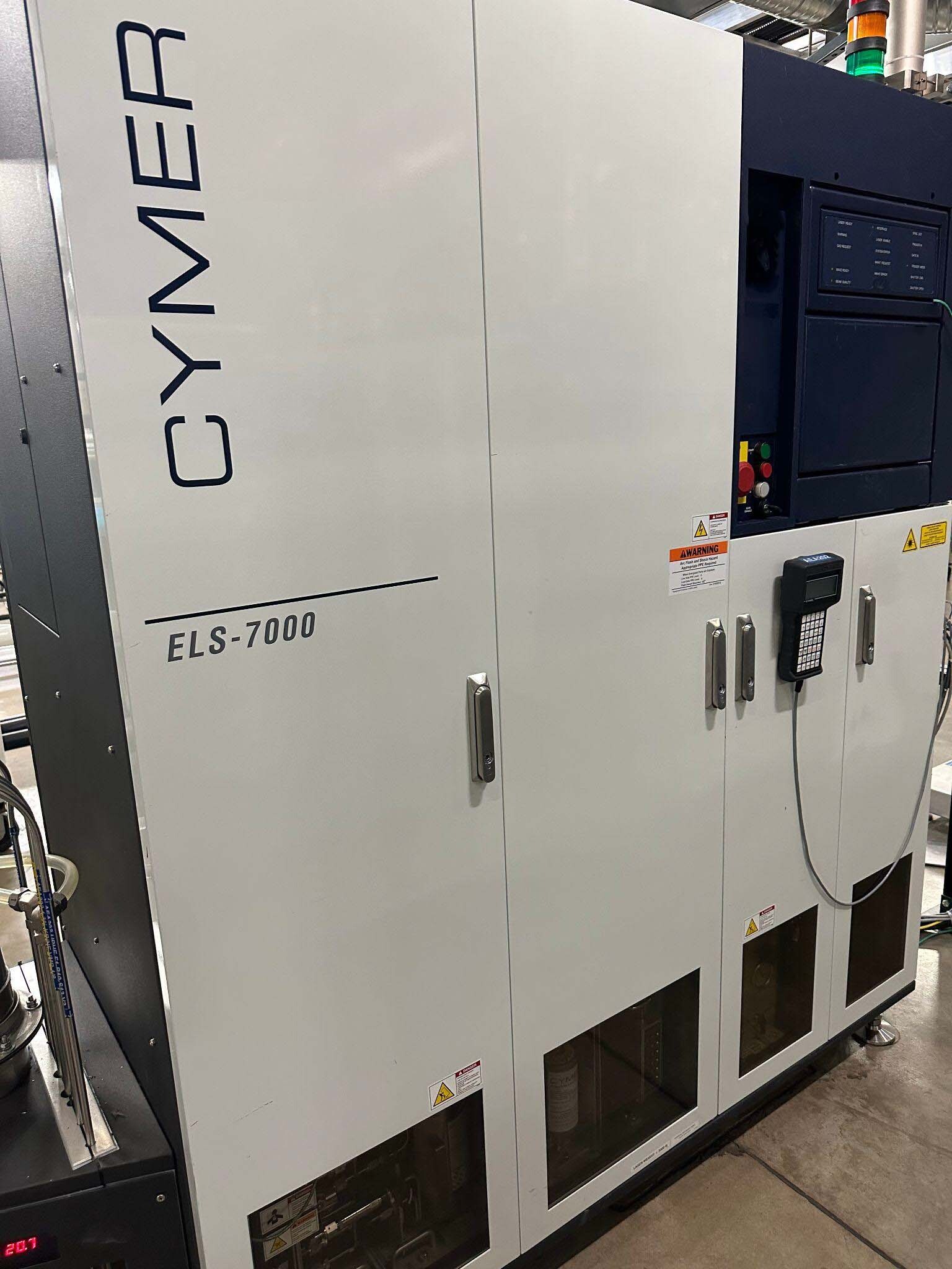
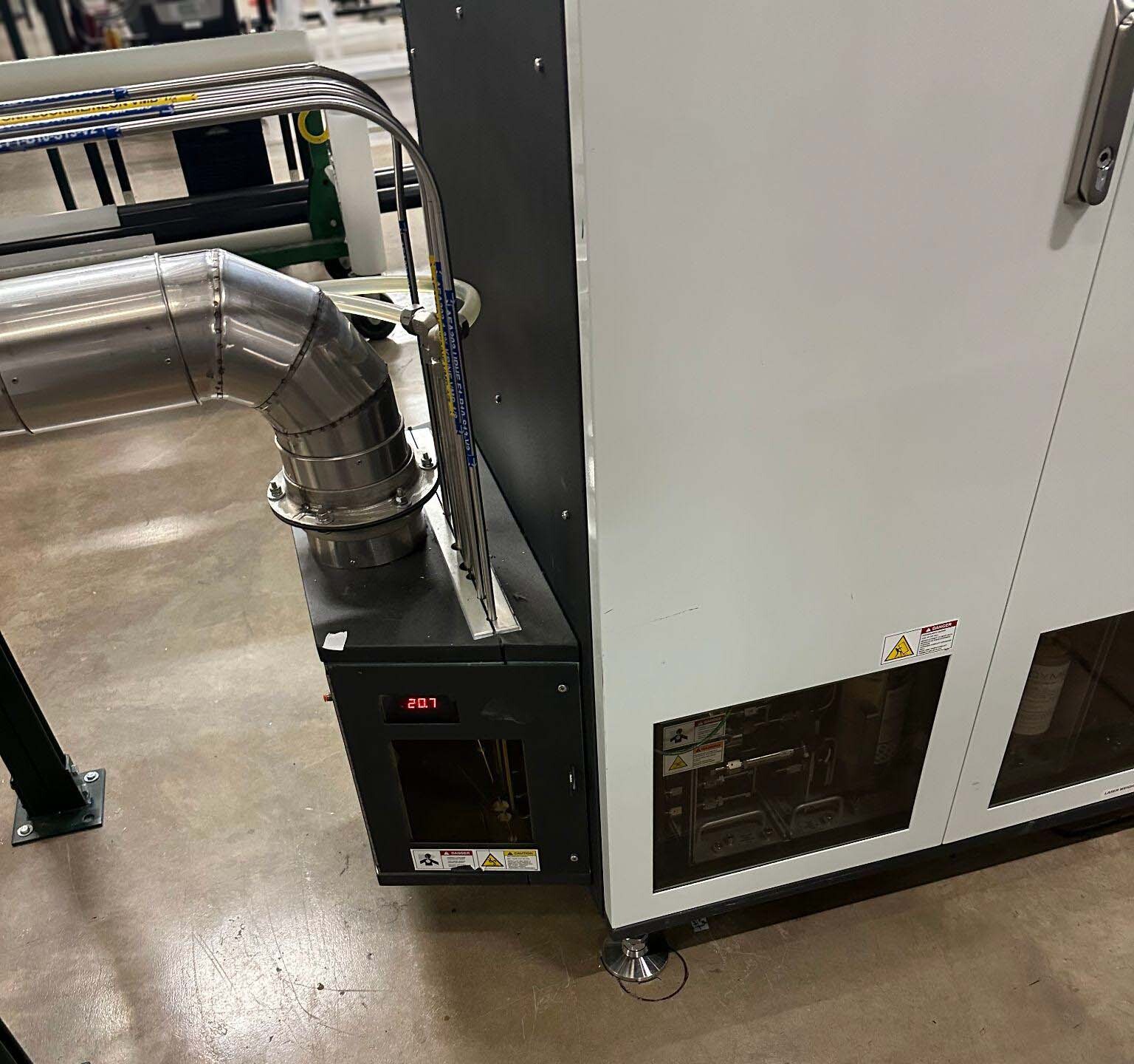
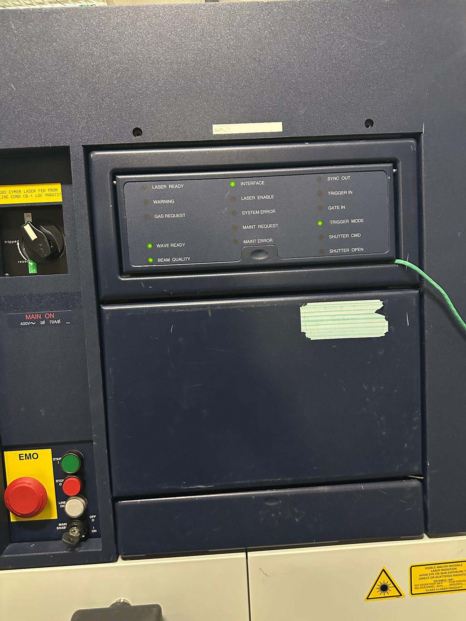
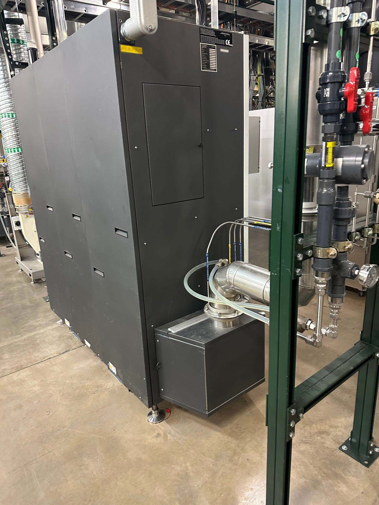
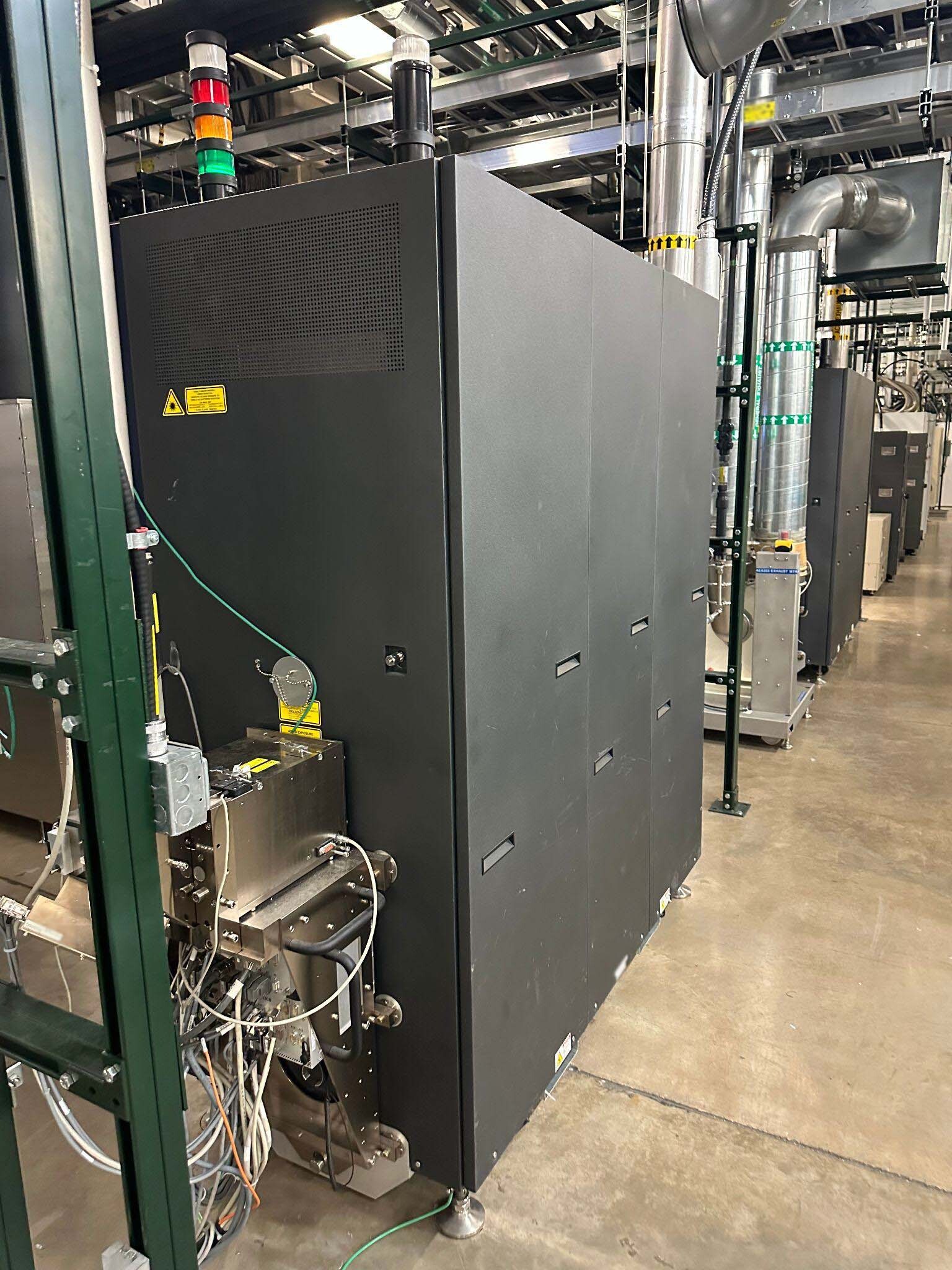
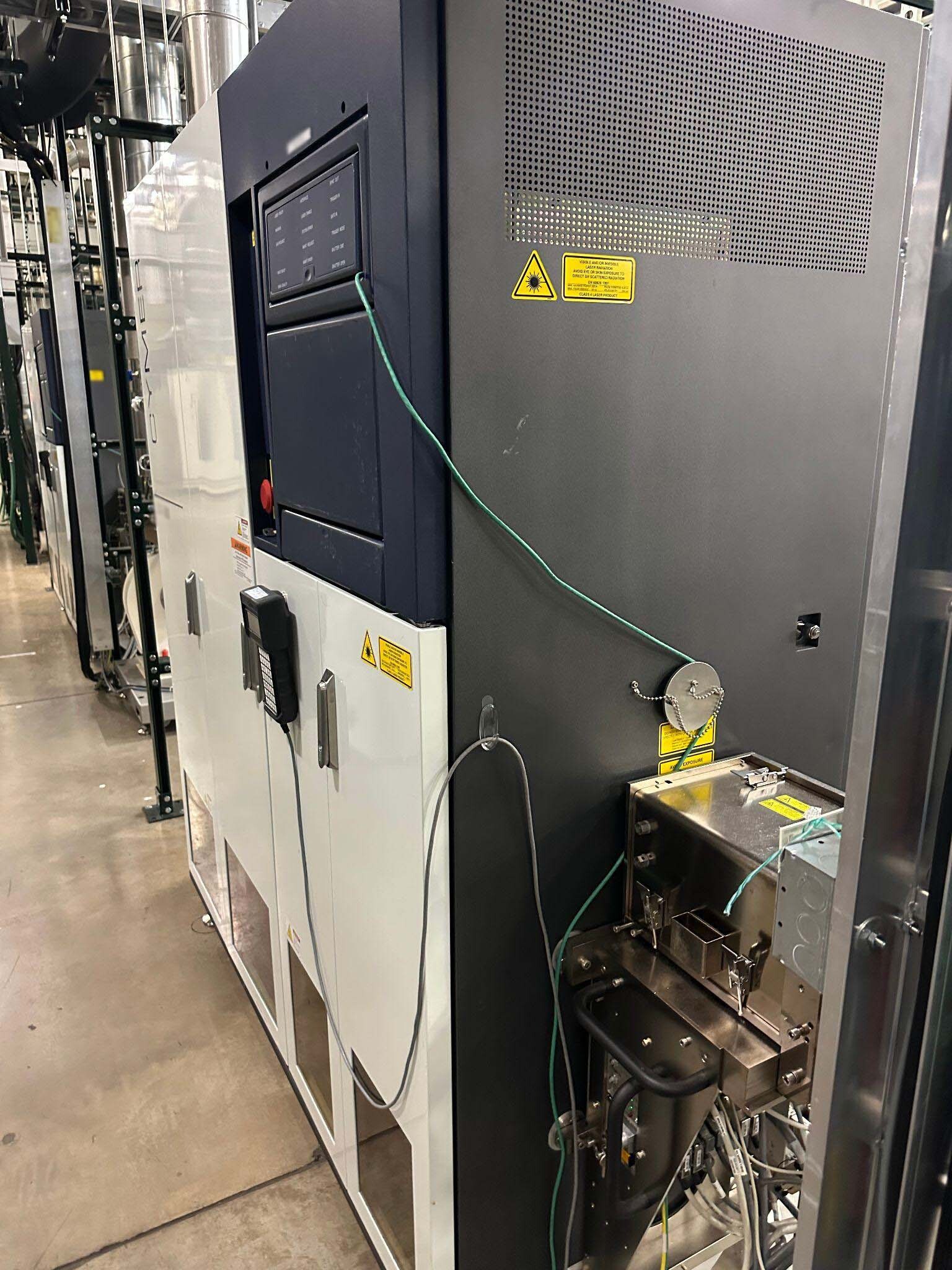
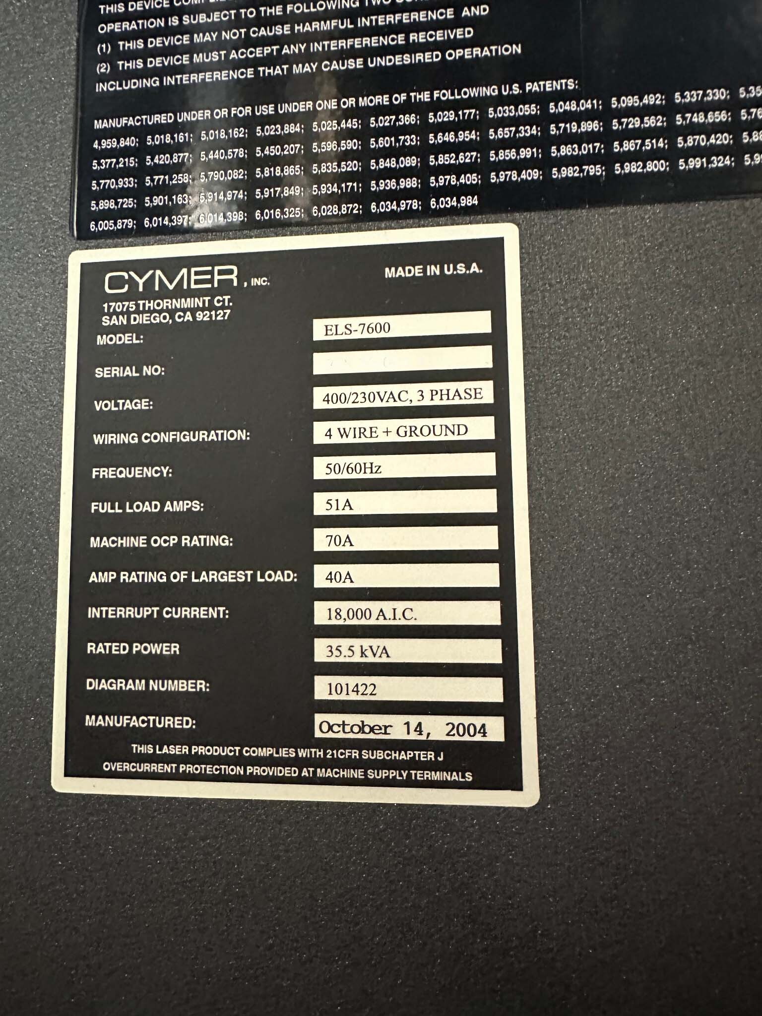
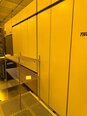
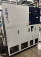
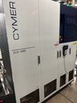
ASML Twinscan 850 is a cutting-edge wafer stepper equipment that plays a pivotal role in the semiconductor industry for producing advanced integrated circuits. This advanced lithography system is designed and manufactured by ASML, a leading provider of photolithography equipment for semiconductor manufacturing. Twinscan 850 incorporates state-of-the-art technology to achieve high-resolution patterning on silicon wafers, enabling the production of smaller and more complex electronic devices. At the heart of the unit is a sophisticated projection lens that is capable of precisely projecting the photomask pattern onto the silicon wafer with extreme accuracy and consistency. One of the key features of ASML Twinscan 850 is its ability to achieve high throughput and productivity while maintaining exceptional image quality. This is achieved through a combination of advanced optics, precise alignment systems, and innovative software algorithms that optimize the lithography process. The machine is equipped with multiple light sources, typically utilizing deep ultraviolet (DUV) light with wavelengths in the range of 193nm to 248nm. These light sources generate the necessary illumination to expose the photoresist on the wafer, allowing for the transfer of the mask pattern onto the silicon substrate. Twinscan 850 also employs a sophisticated stage tool that moves the silicon wafer in small, precise increments to ensure accurate alignment and overlay between successive layers of the chip. This stage asset is equipped with advanced sensors and feedback mechanisms to monitor and control the position of the wafer in real-time during exposure. Furthermore, the model incorporates advanced aberration correction technology to compensate for optical distortions and imperfections in the projection lens, ensuring that the final pattern on the wafer is faithful to the original design. In addition, ASML Twinscan 850 features a highly automated operation with software-controlled processes for mask loading, alignment, exposure, and unloading. This automation not only enhances productivity but also reduces the potential for human error and variability in the lithography process. Furthermore, the equipment is designed to be compatible with various types of photomasks, including binary, phase-shift, and attenuated phase-shift masks, allowing semiconductor manufacturers to utilize different patterning techniques to achieve the desired circuit layout on the silicon wafer. Overall, Twinscan 850 represents a state-of-the-art wafer stepper system that is essential for achieving the high-resolution patterning required for advanced semiconductor devices. With its advanced optics, precise alignment systems, and automated operation, this lithography unit enables semiconductor manufacturers to push the boundaries of chip design and fabrication, driving innovation in the electronics industry.
There are no reviews yet