Used ASML Twinscan AT 1250 #293817993 for sale
URL successfully copied!





Tap to zoom
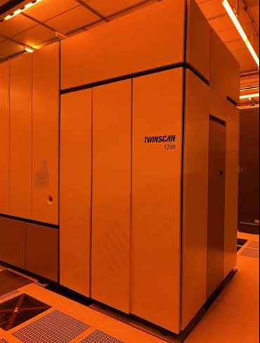

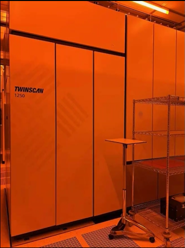
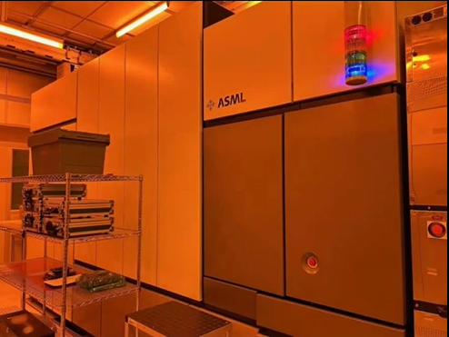
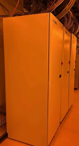
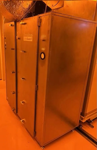
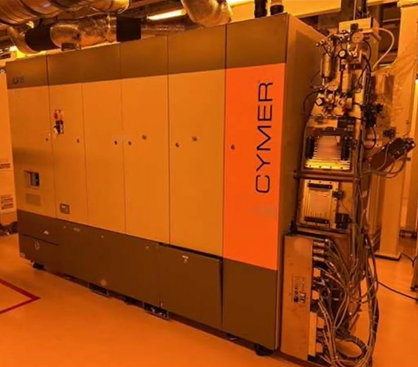
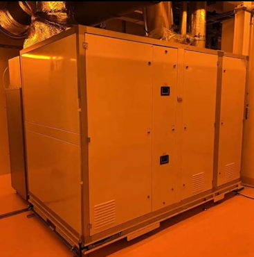
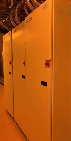
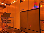
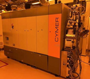
ASML Twinscan AT 1250 is a cutting-edge semiconductor wafer stepper used in the photolithography process in semiconductor manufacturing. As one of the flagship models from ASML, a leading supplier of photolithography equipment, the AT 1250 embodies state-of-the-art technology and advanced capabilities to enable high-resolution patterning on silicon wafers. The AT 1250 features a dual-stage design with two independent stages that move independently to enhance throughput and overlay performance. This design allows for continuous exposure and stage swapping, minimizing downtime and maximizing productivity in high-volume manufacturing environments. The equipment is equipped with advanced alignment and calibration capabilities to ensure precise overlay control, critical for achieving submicron resolution requirements in leading-edge semiconductor processes. One of the key highlights of the AT 1250 is its projection lens system, which plays a crucial role in determining the unit's resolution, field size, and overall performance. The machine utilizes a sophisticated lens design optimized for resolution and aberration control, enabling the projection of high-fidelity patterns onto the wafer with exceptional clarity and precision. The lens tool is complemented by advanced illumination sources and optical components that work in concert to deliver superior imaging performance across a wide range of patterning requirements. In terms of specifications, the AT1250 offers a configurable resolution down to sub-10-nanometer levels, making it suitable for manufacturing advanced semiconductor devices with complex geometries and tight design rules. The asset supports multiple wavelength options, including deep ultraviolet (DUV) and extreme ultraviolet (EUV) lithography, enabling flexibility in addressing diverse patterning needs across different technology nodes. The AT 1250 is designed with a comprehensive suite of automation features to streamline operation and enhance model reliability. The equipment integrates advanced process control algorithms and metrology capabilities to enable in-situ monitoring and real-time adjustments, ensuring consistent patterning performance and yield optimization. Additionally, the system is equipped with intelligent self-diagnostic tools and remote monitoring capabilities to facilitate proactive maintenance and minimize downtime in high-volume manufacturing environments. With a focus on sustainability and cost-effectiveness, the AT 1250 incorporates energy-efficient components and smart power management features to minimize power consumption and reduce the overall environmental footprint of semiconductor manufacturing operations. The unit is designed for optimal uptime and operational efficiency, with robust components and advanced cooling systems to support continuous operation in demanding fabrication environments. In conclusion, Twinscan AT 1250 represents a state-of-the-art solution for advanced semiconductor lithography, combining cutting-edge technology, high-performance capabilities, and operational robustness to meet the evolving requirements of the semiconductor industry. As a flagship model from ASML, the AT 1250 sets new standards for precision, productivity, and process control in semiconductor manufacturing, empowering chipmakers to push the boundaries of innovation and drive progress in semiconductor technology.
There are no reviews yet