Used ASML Twinscan AT 850D #293758540 for sale
URL successfully copied!







Tap to zoom
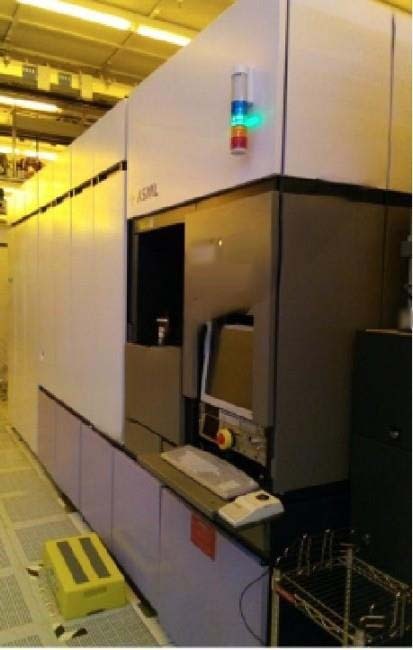

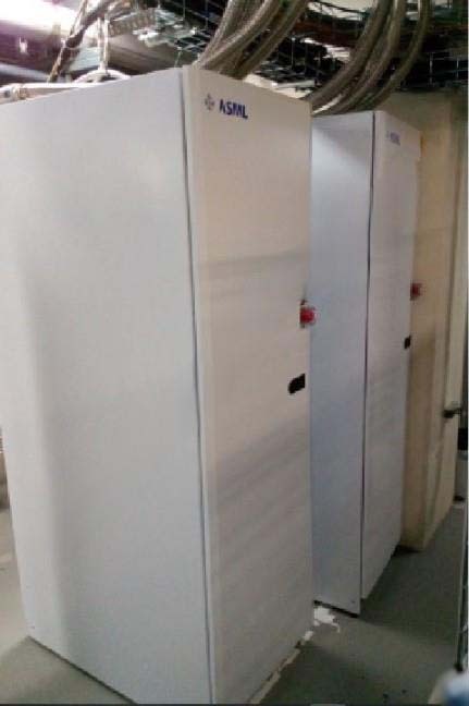
ID: 293758540
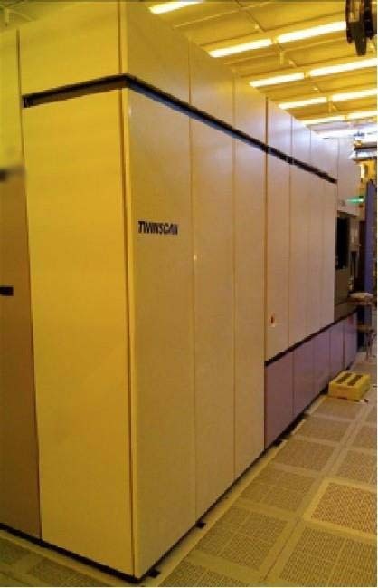
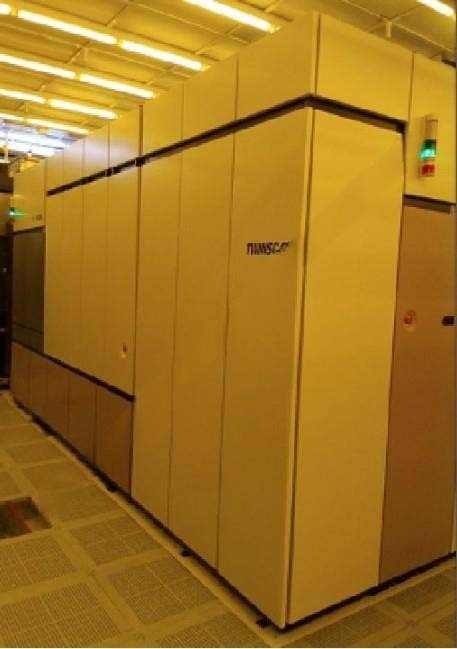
Scanner
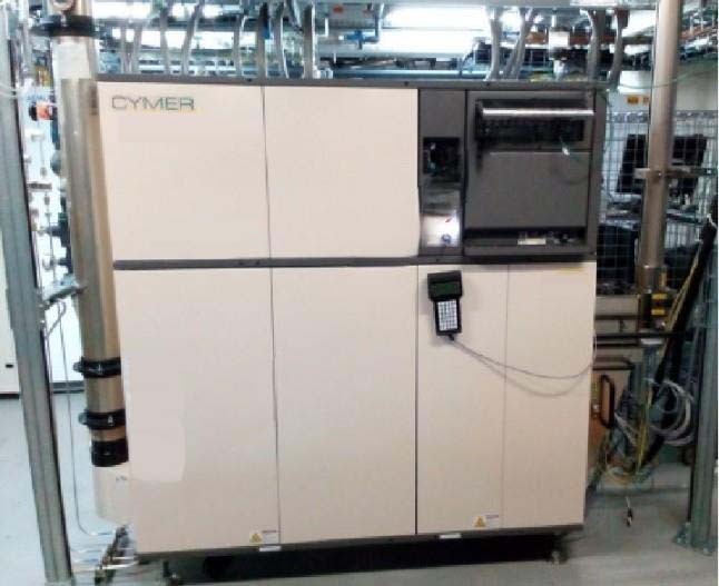
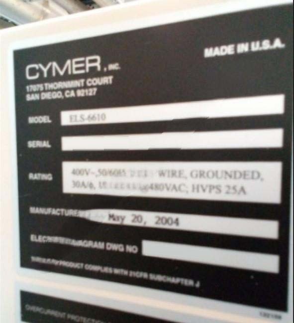
CYMER ELS-6610 Laser
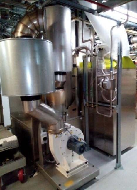
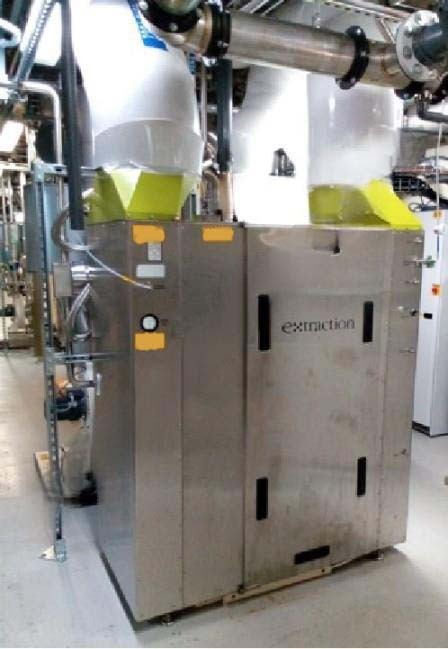
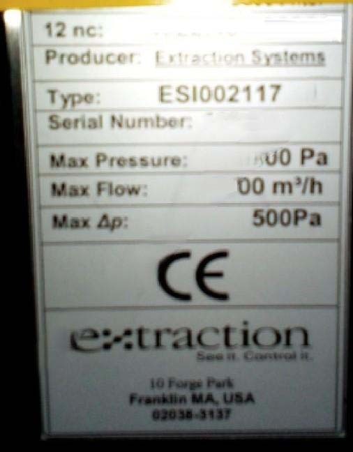
EXTRACTION ESI002117 System
Hard Disk Drive (HDD)
(2) Mini-burl tables
Top-2
Spotless
Cabinets:
ACC
LCWC
MCWC
MDC
Power supply: 400 V, 3 Phase.
ASML Twinscan AT 850D is a state-of-the-art wafer stepper designed by ASML, a leading manufacturer of photolithography equipment used in semiconductor manufacturing. This advanced equipment is part of the Twinscan platform, renowned for its high precision, throughput, and reliability in producing integrated circuits with ever-shrinking feature sizes. At the core of the AT 850D wafer stepper is its advanced projection lens system, which plays a crucial role in achieving ultra-high resolution and accuracy in patterning semiconductor wafers. The unit utilizes immersion lithography technology, where a liquid medium, typically purified water, is used to enhance the imaging performance, enabling the projection of smaller features onto the wafer surface. The AT 850D features a dual-stage design, consisting of a wafer stage and a reticle stage, that allows for independent motion and control of the wafer and the reticle during the exposure process. This dual-stage architecture enables high-speed scanning of the reticle pattern across the wafer, minimizing exposure time and maximizing productivity in semiconductor fabrication. One of the key highlights of the AT 850D is its ability to support multiple patterning techniques, such as double patterning and multipatterning, to achieve sub-10nm resolution capabilities required for cutting-edge semiconductor devices. The machine is equipped with advanced overlay control mechanisms to ensure precise alignment of multiple patterning layers, critical for achieving the desired device performance and yield. In addition, the AT 850D incorporates sophisticated adaptive optics technology to compensate for lens aberrations and other optical distortions, ensuring optimal image quality and pattern fidelity across the entire wafer surface. The tool is also equipped with advanced illumination control features, including adjustable numerical aperture and illumination modes, to optimize imaging performance for different lithography processes. The AT 850D boasts a high throughput capability, thanks to its advanced stage technology and optimized wafer handling systems. The asset is designed to minimize downtime between exposure shots, allowing for continuous operation and maximizing wafer throughput in high-volume production environments. Moreover, the AT 850D is built with a robust environmental control model to maintain precise temperature and humidity conditions within the exposure chamber, essential for ensuring consistent lithography performance and minimizing process variations. The equipment also features advanced in-situ metrology capabilities for real-time monitoring of critical process parameters, enabling proactive process control and defect reduction. In conclusion, Twinscan AT 850D represents a cutting-edge solution for advanced semiconductor lithography, offering unparalleled resolution, accuracy, and productivity for the production of next-generation integrated circuits. With its advanced optics, dual-stage architecture, multiple patterning support, and high-throughput capabilities, the AT 850D is well-suited for driving innovation and pushing the boundaries of semiconductor technology in the fast-paced industry landscape.
There are no reviews yet