Used ASML Twinscan AT 850D #293799740 for sale
URL successfully copied!


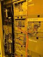
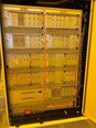
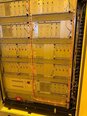
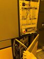
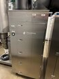
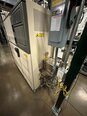
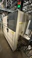
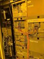


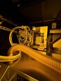
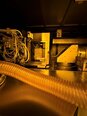
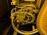
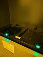


Tap to zoom
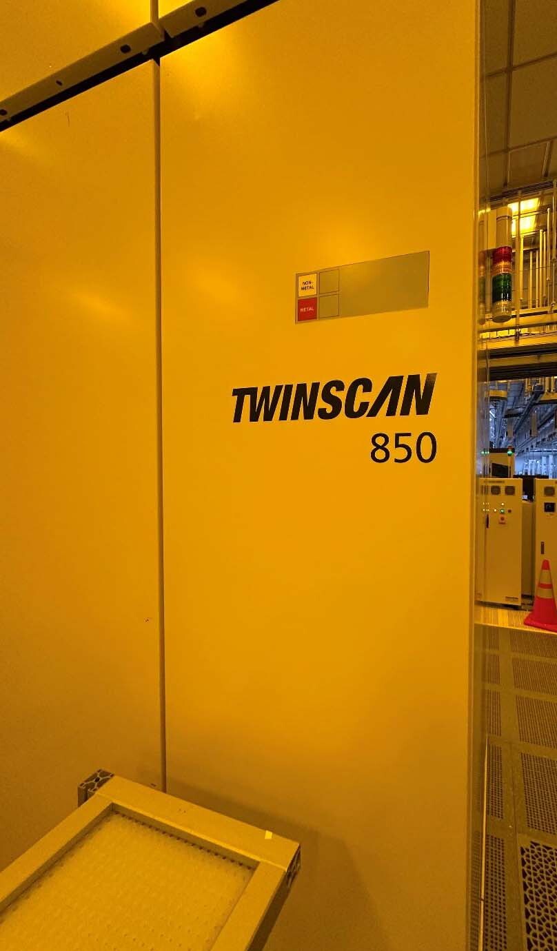

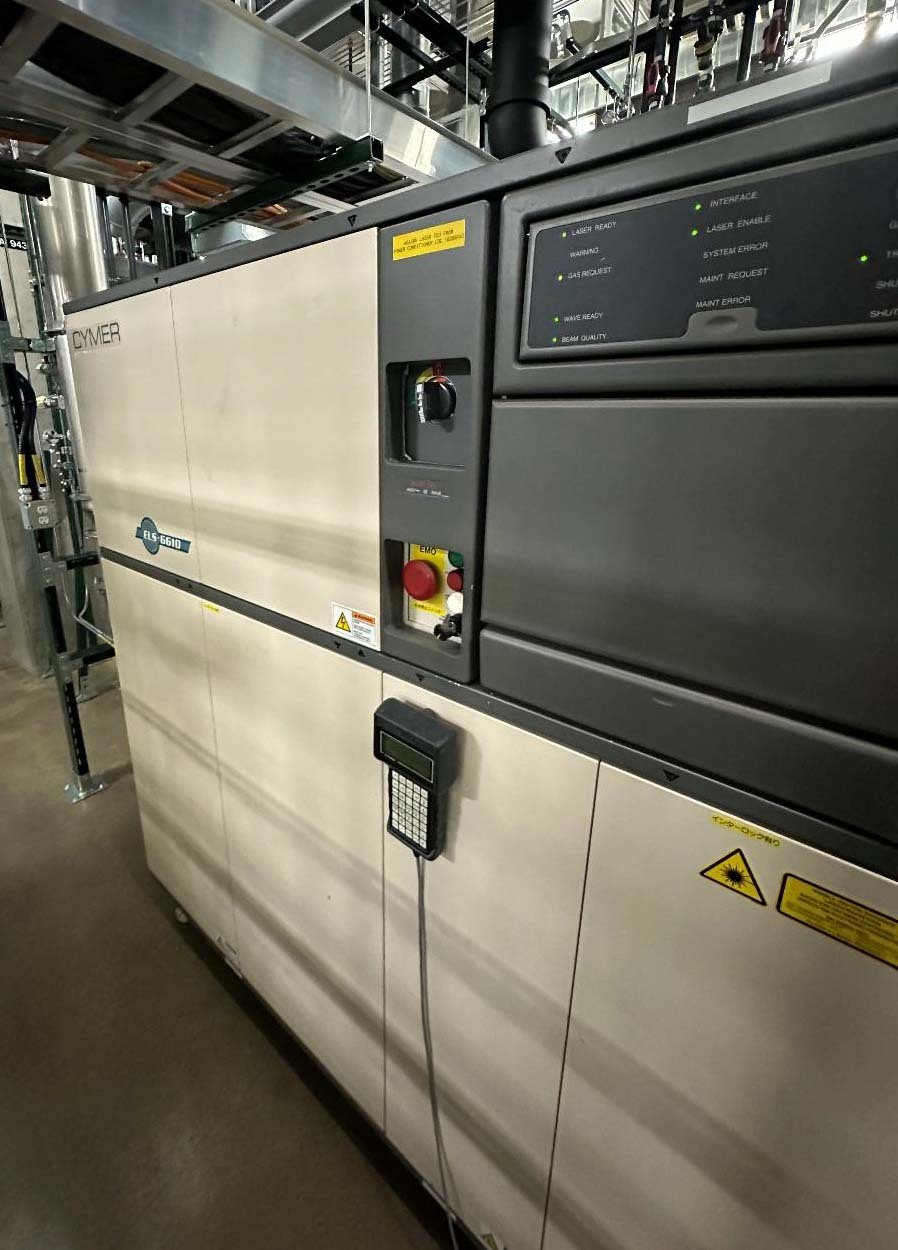
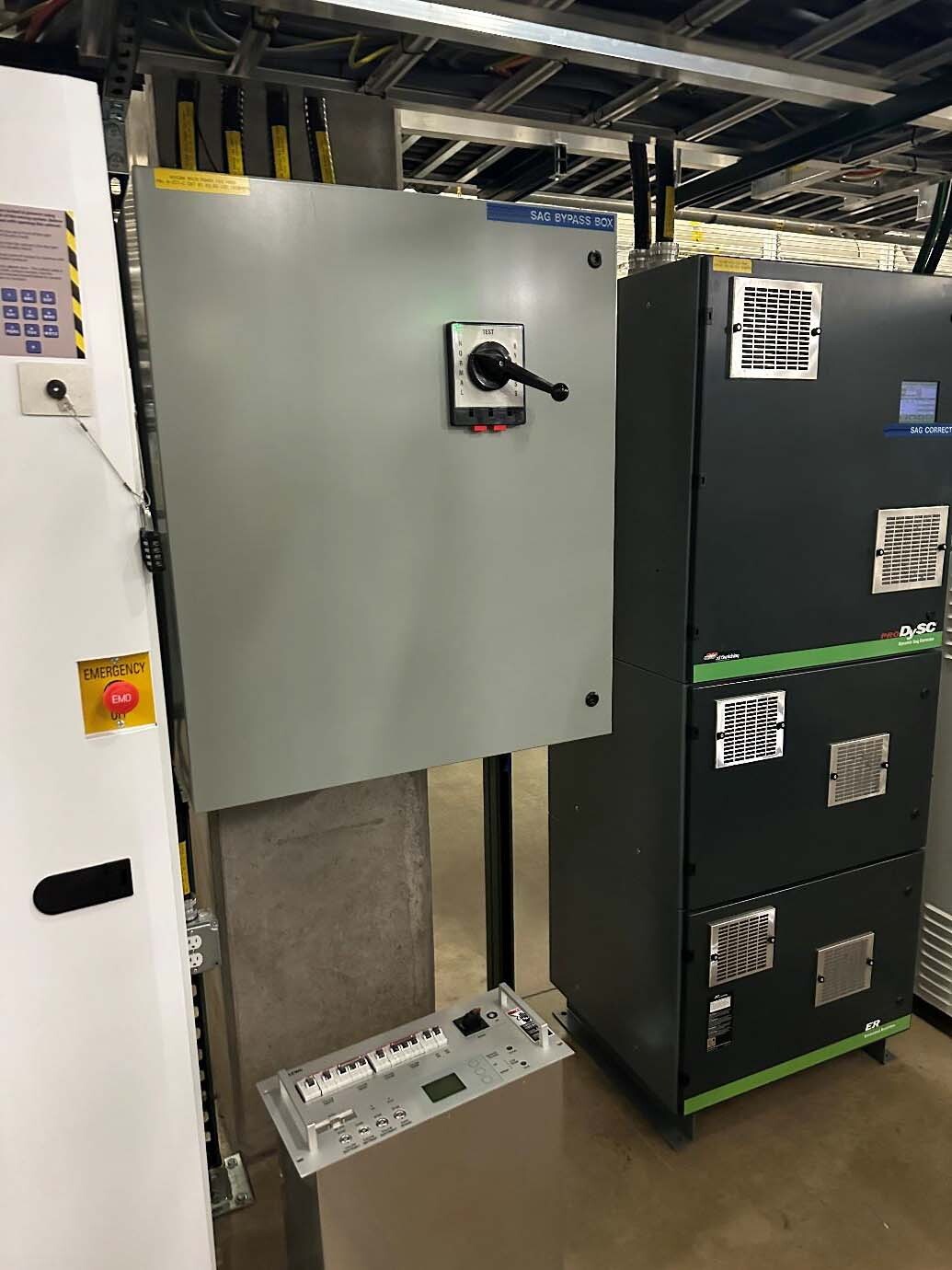
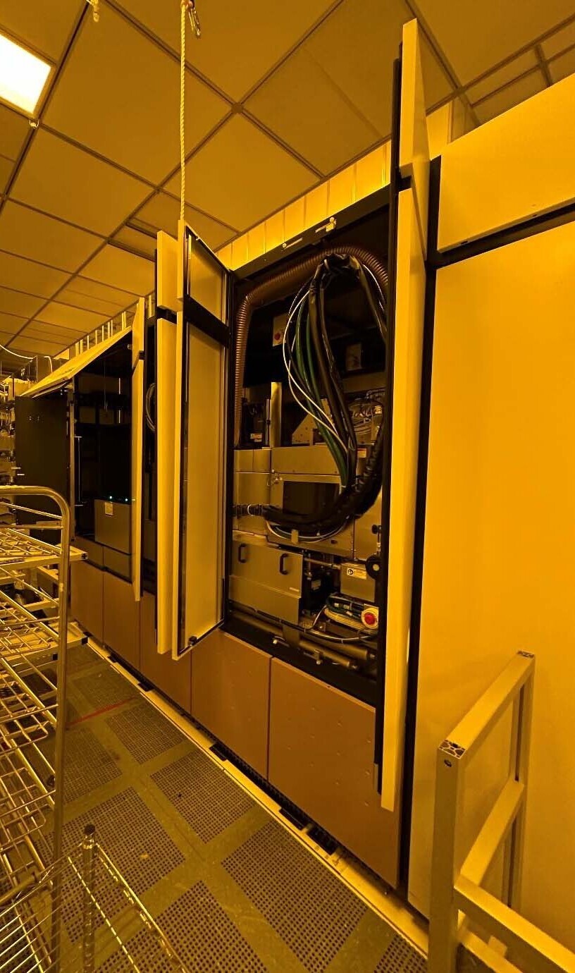
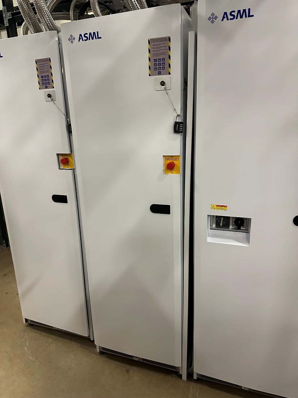
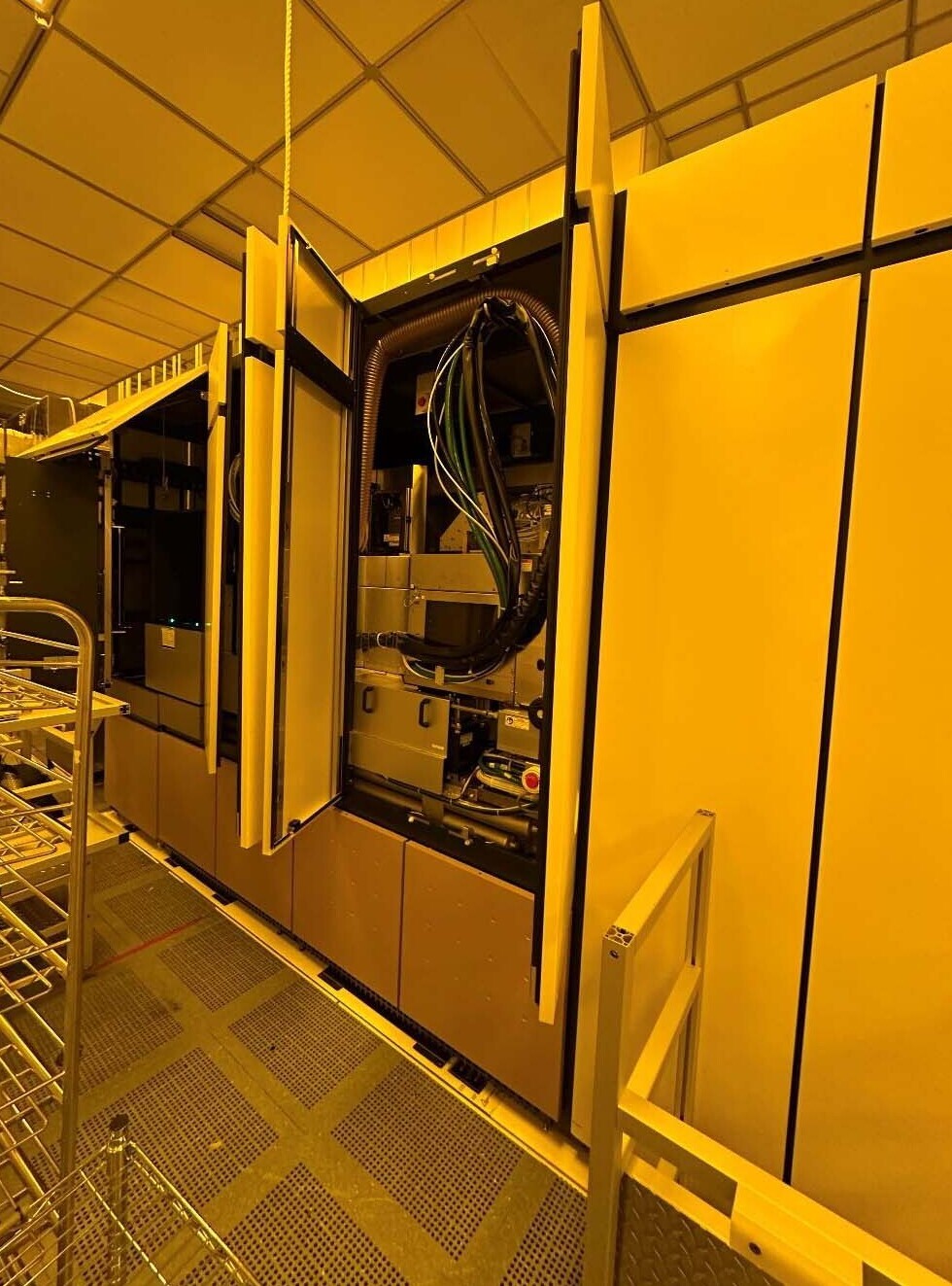
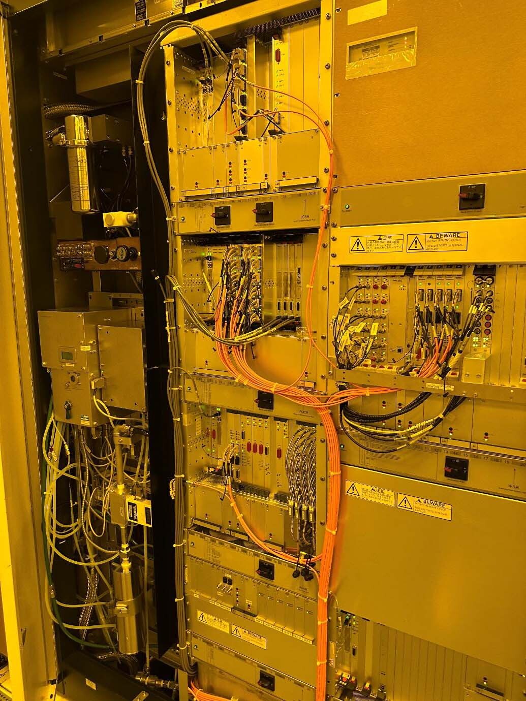
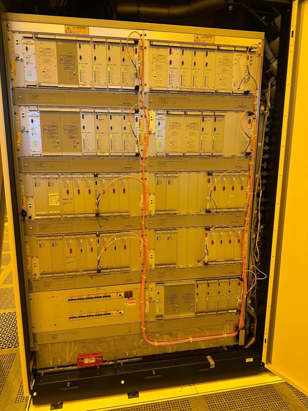
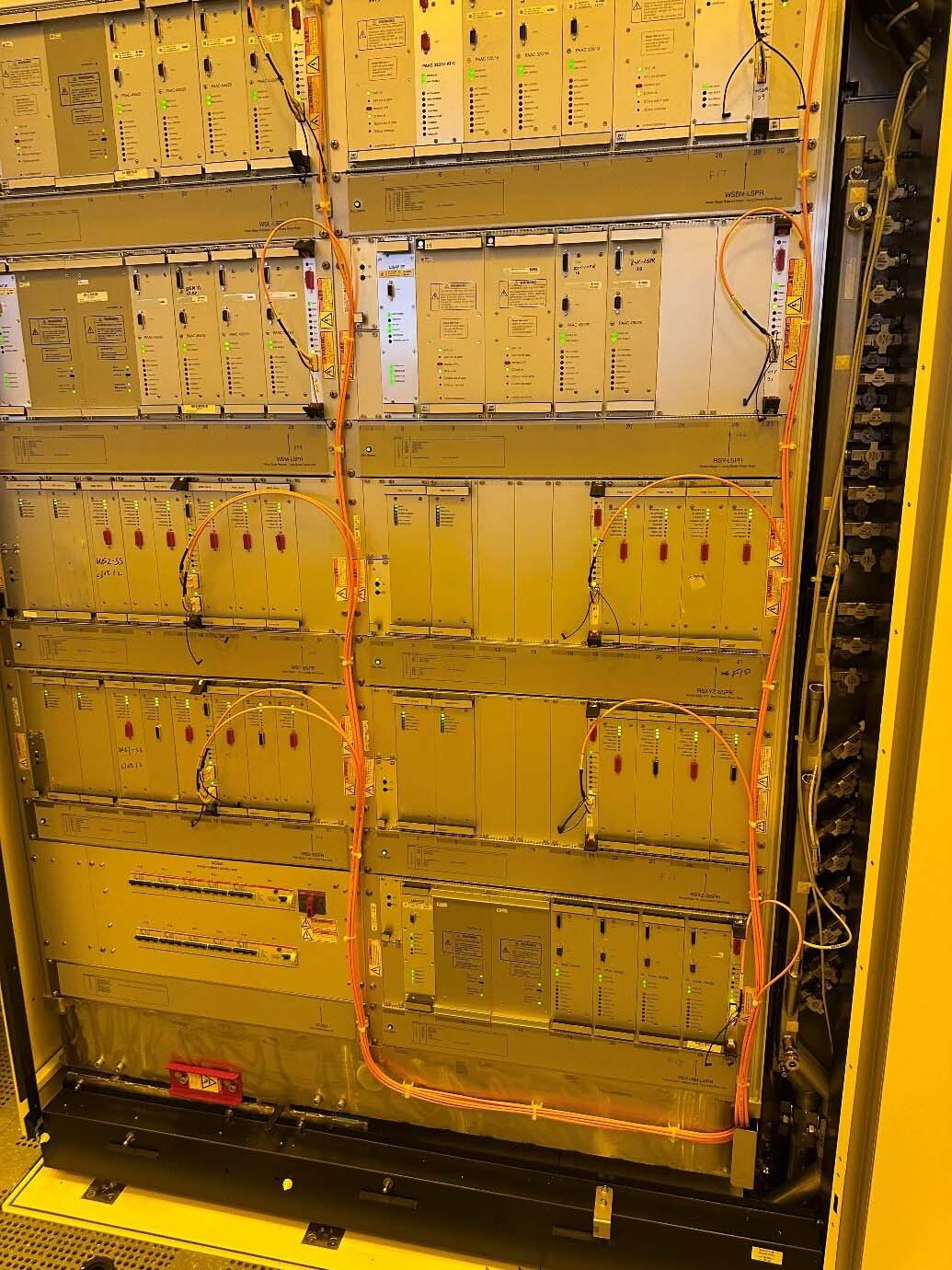
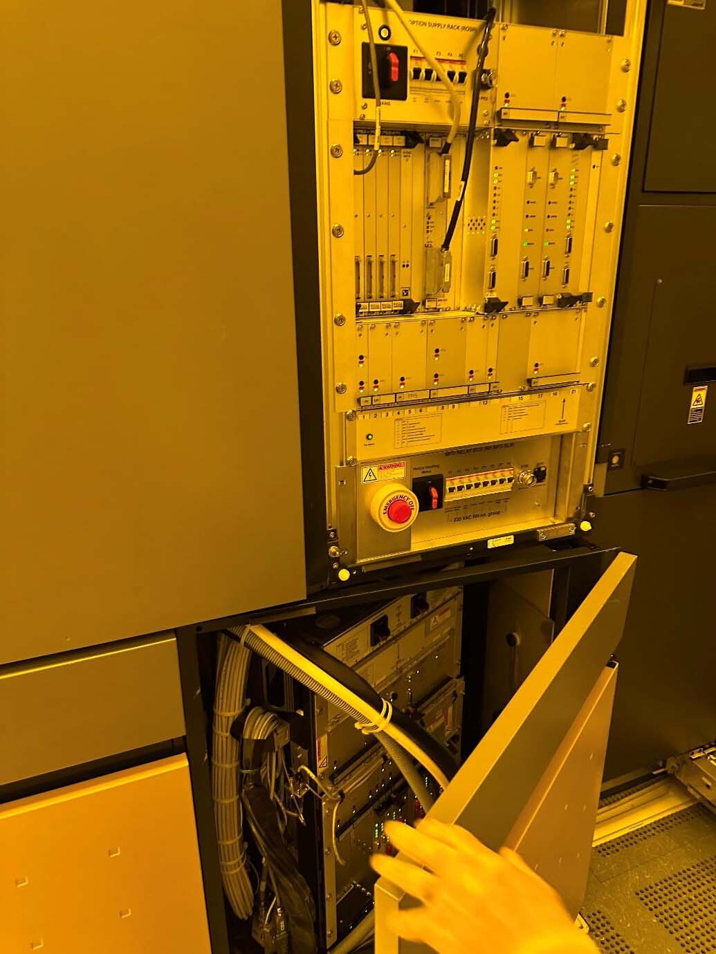
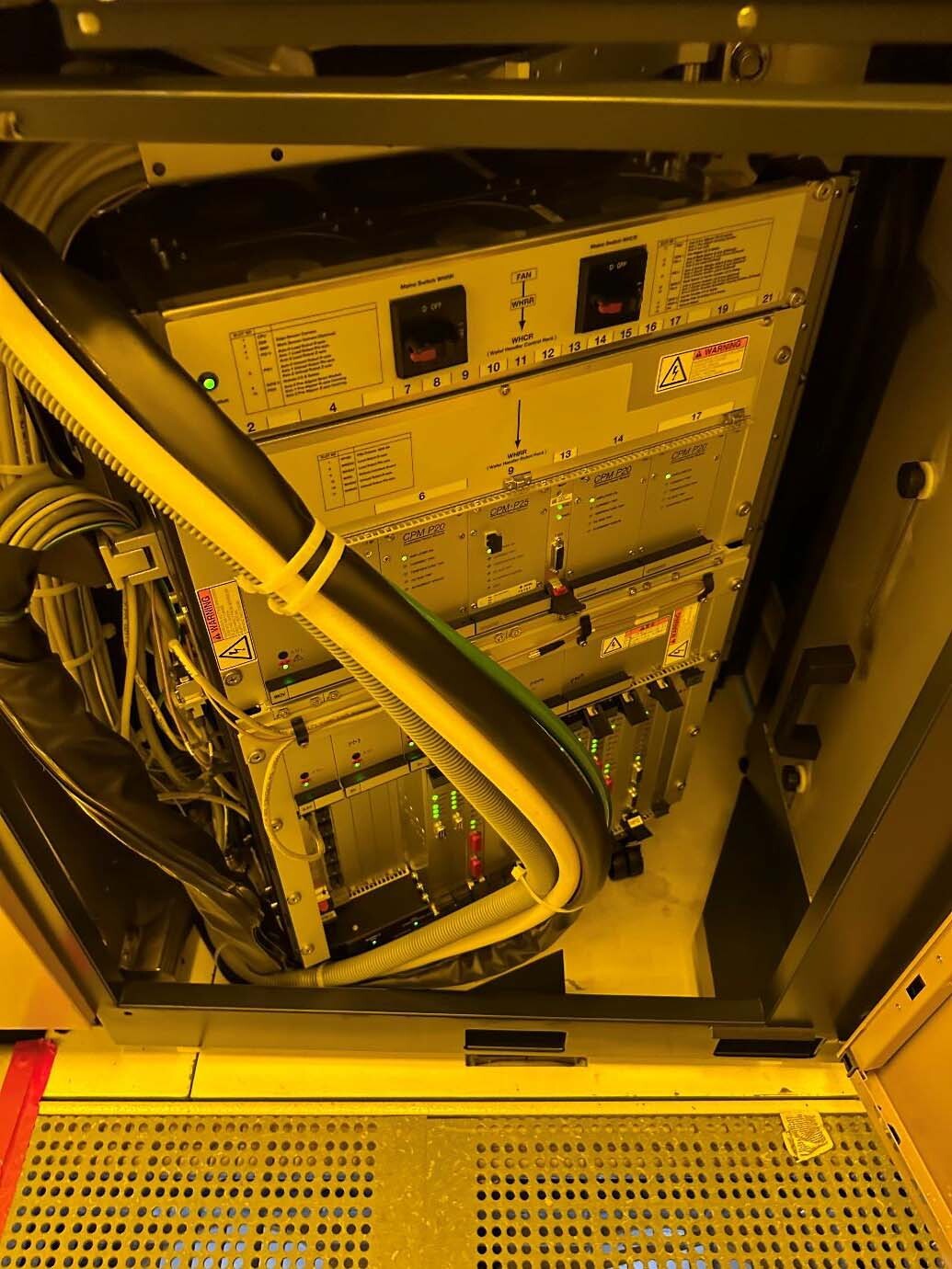
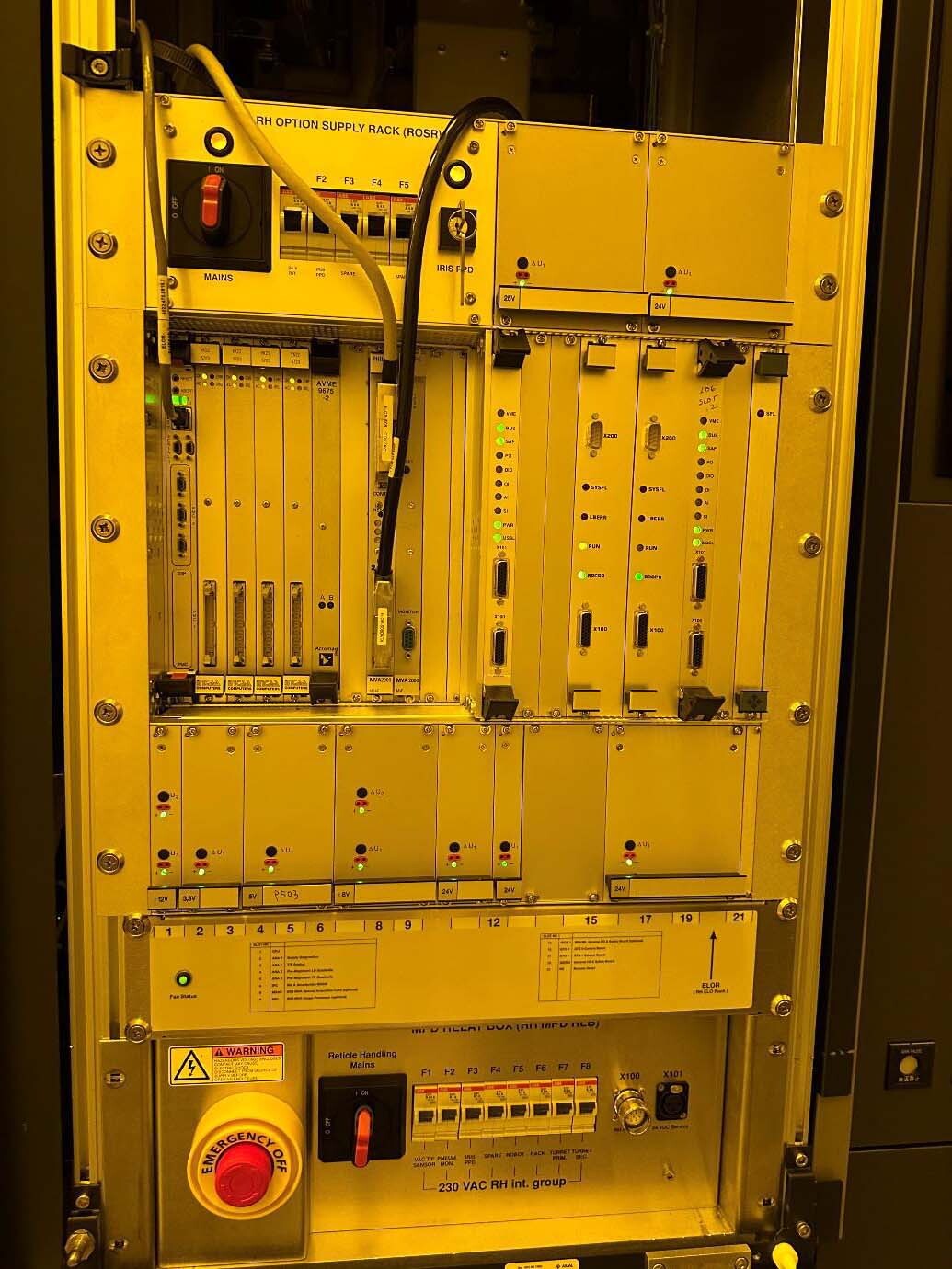
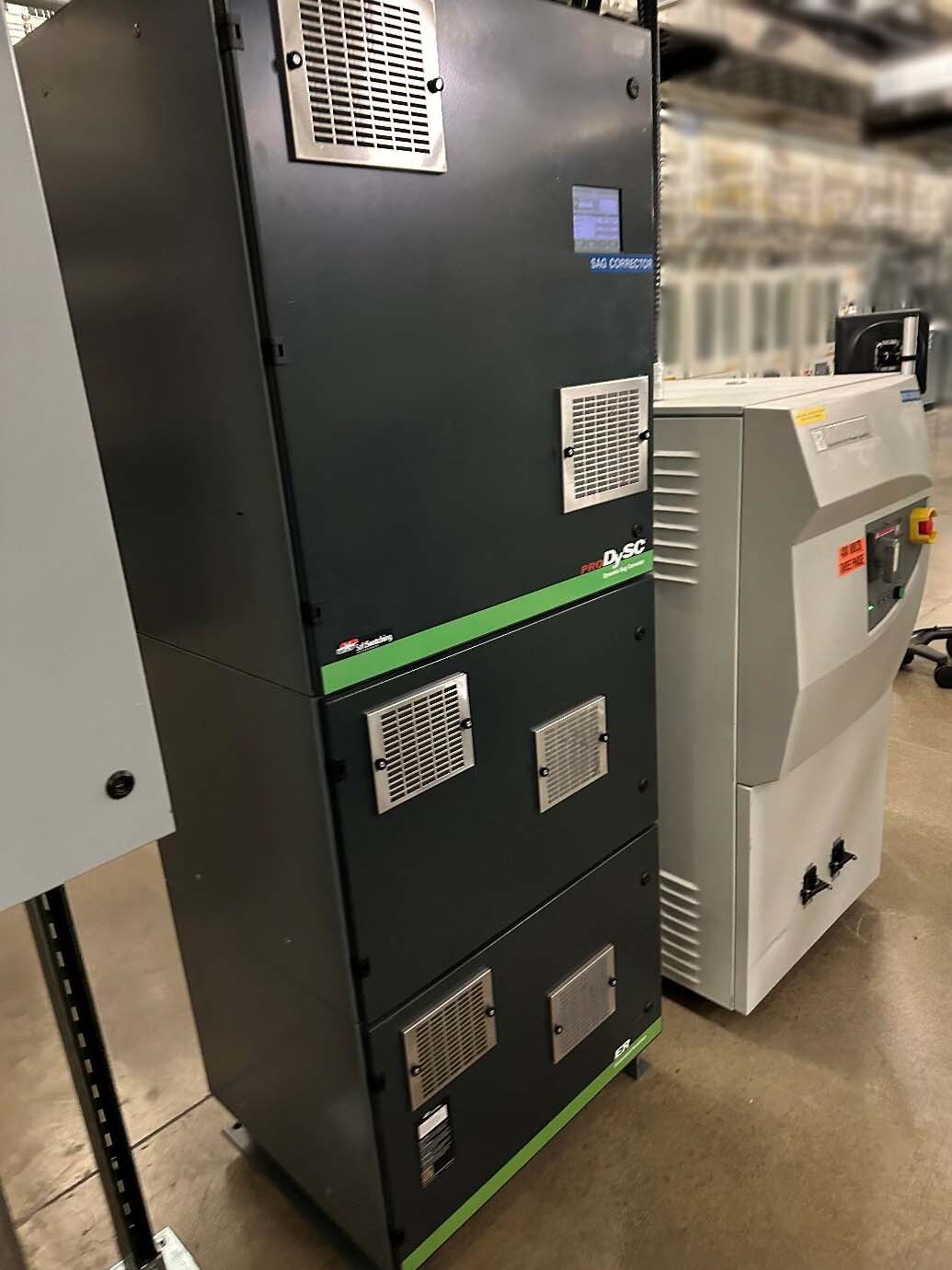
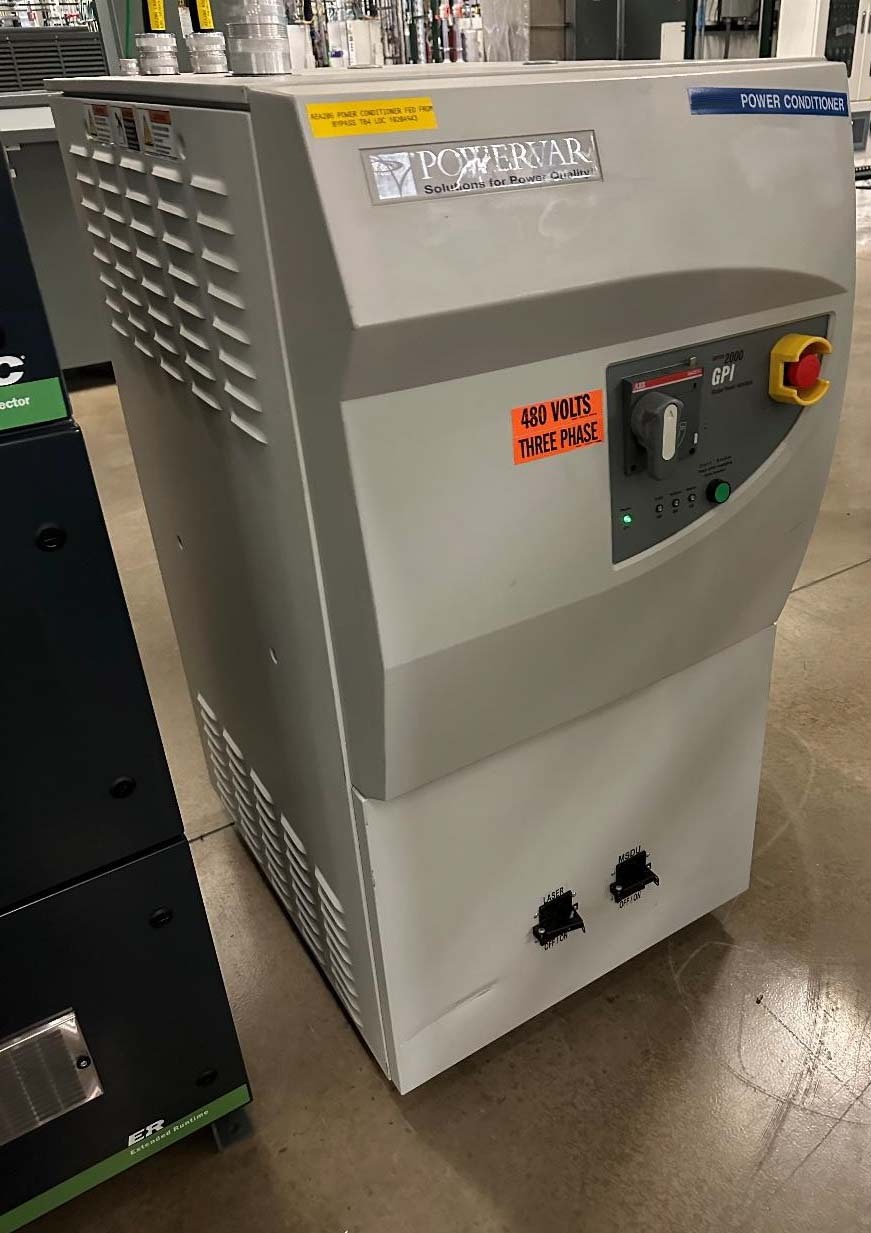
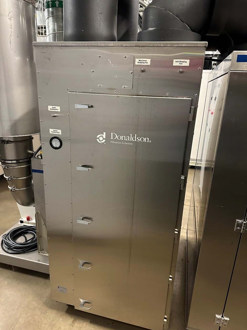
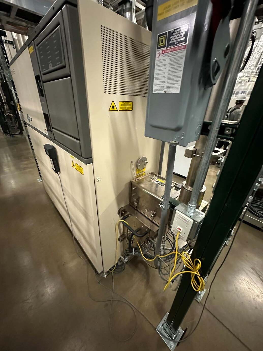
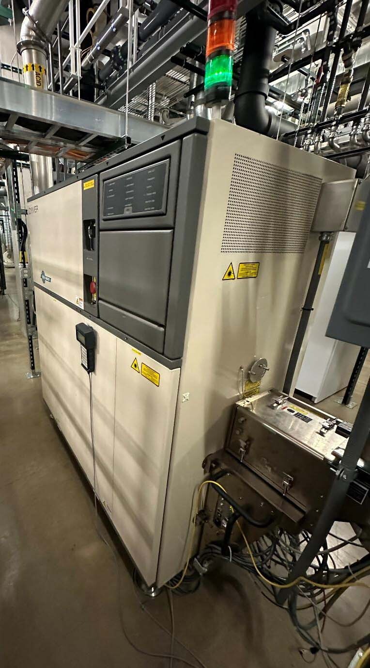
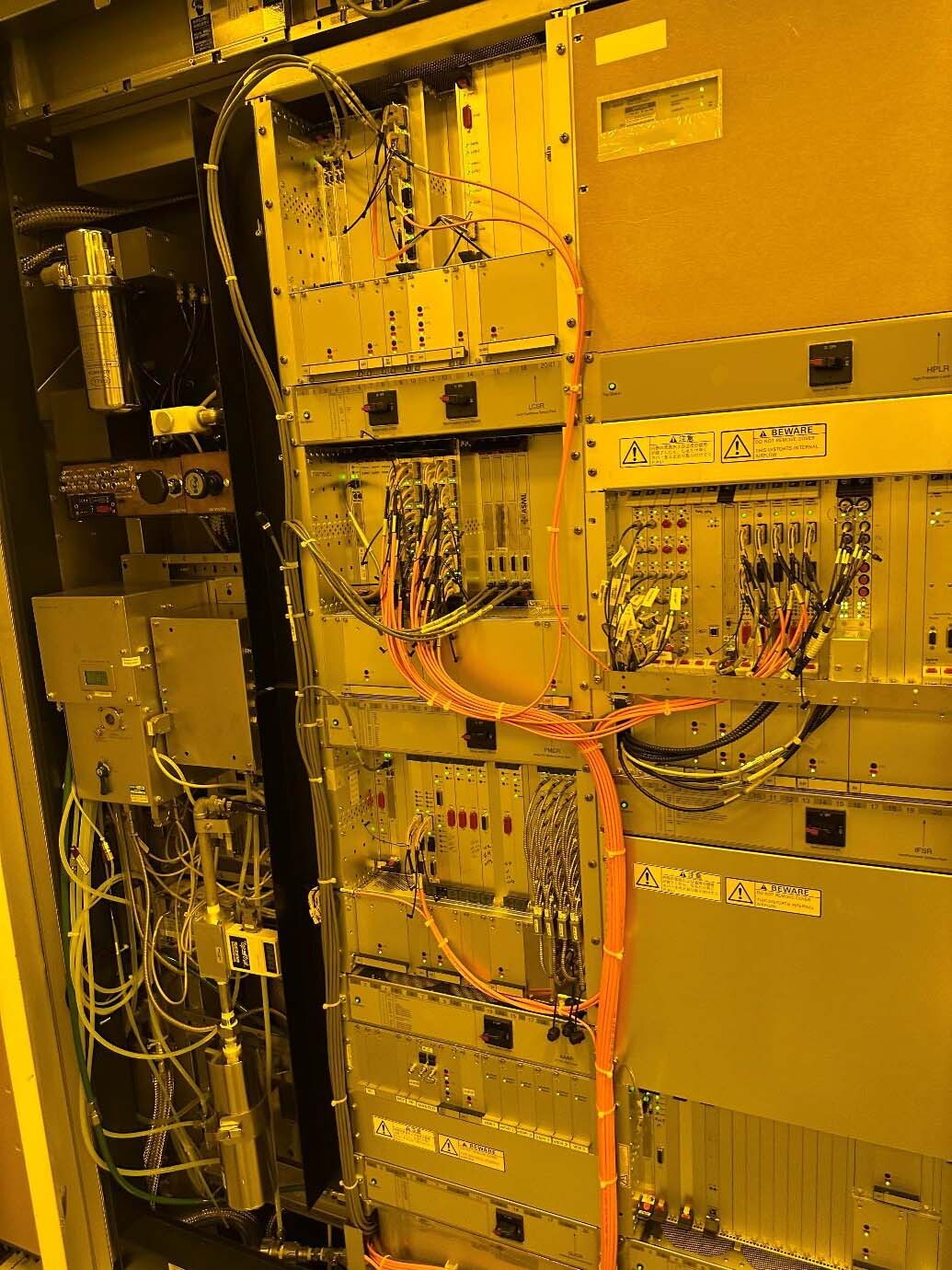
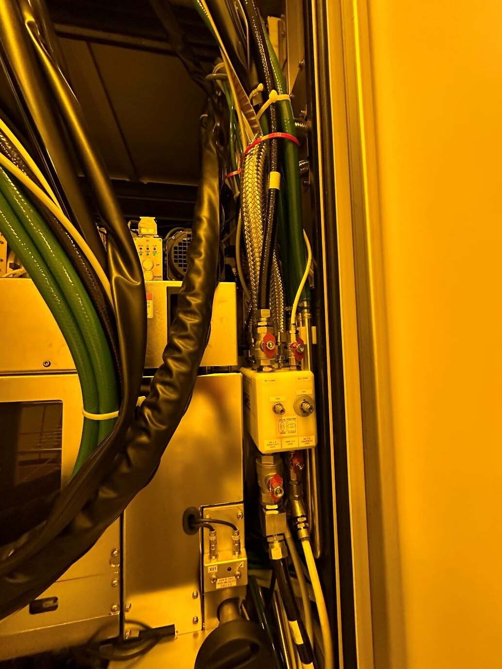
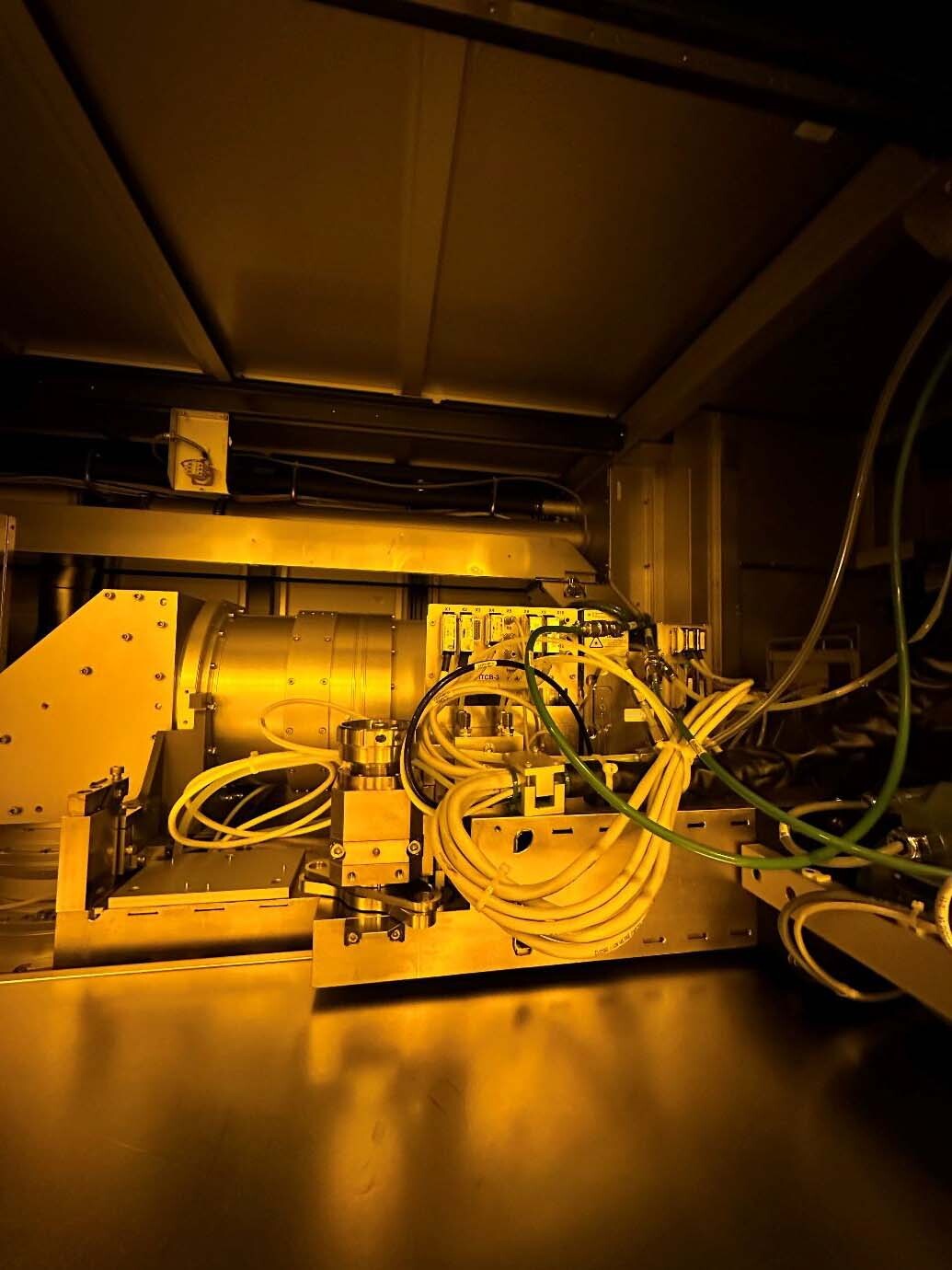
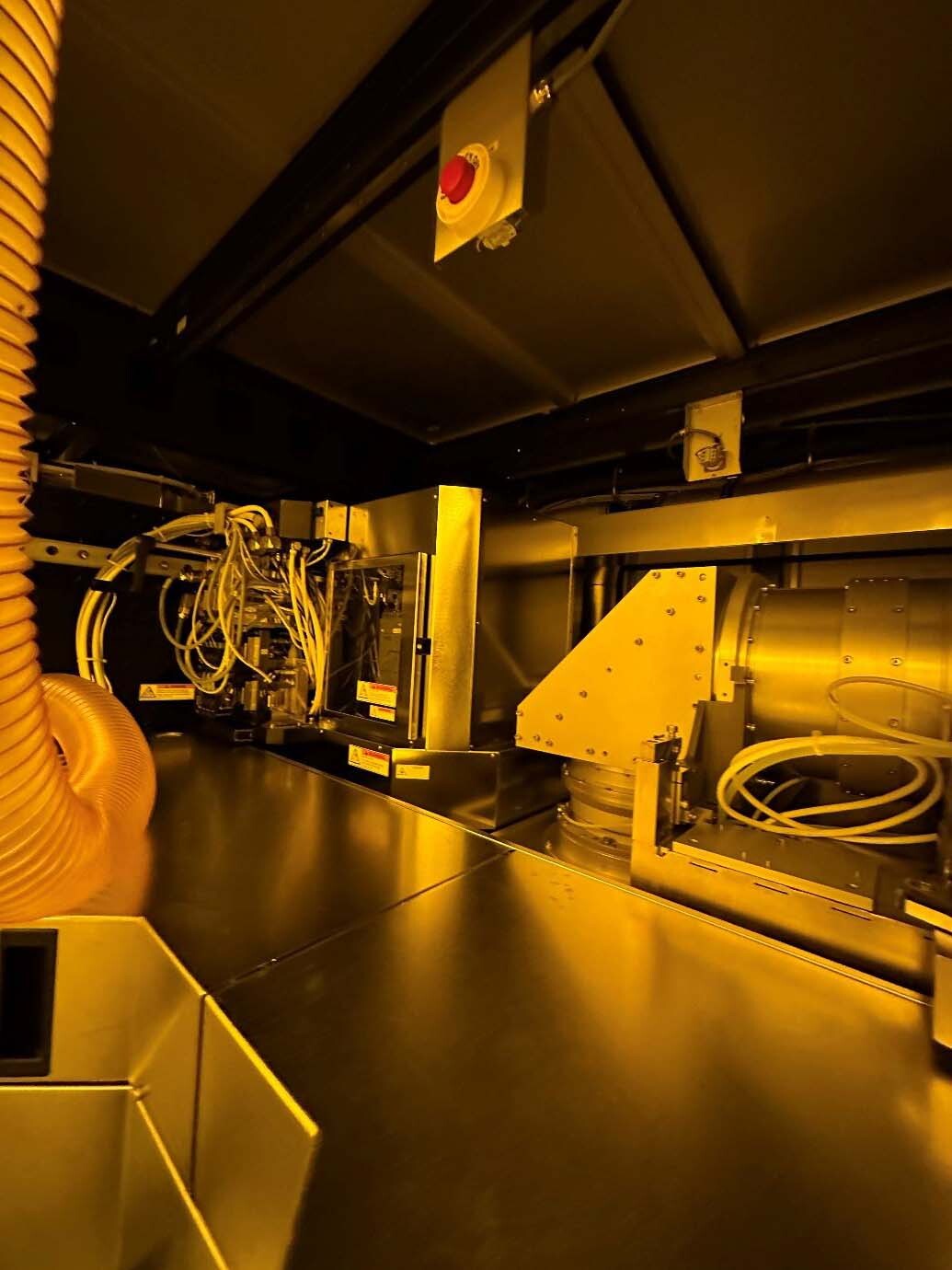
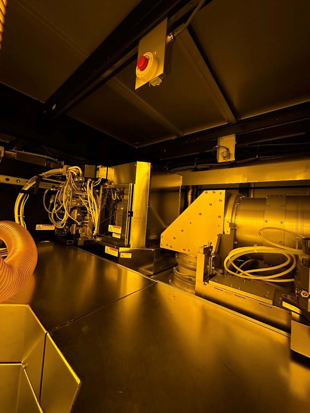
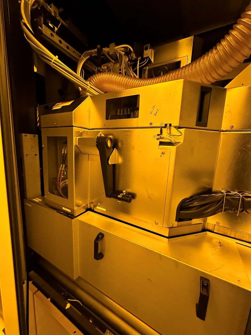
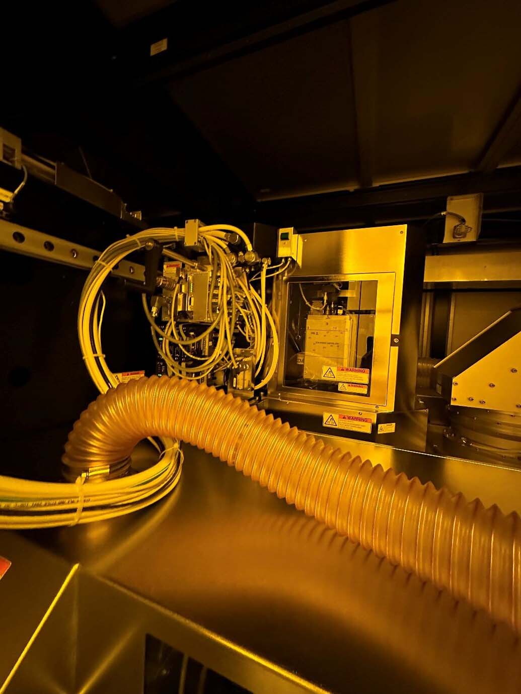
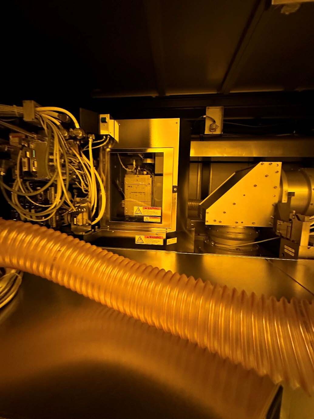
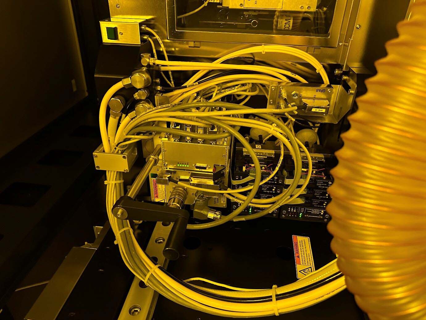
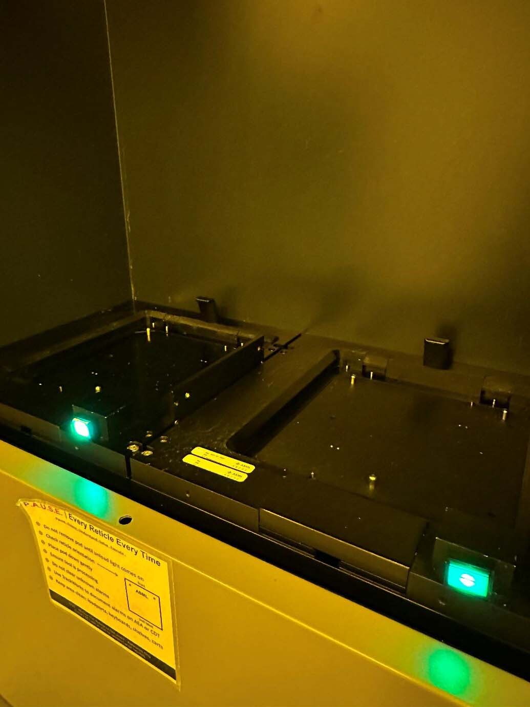
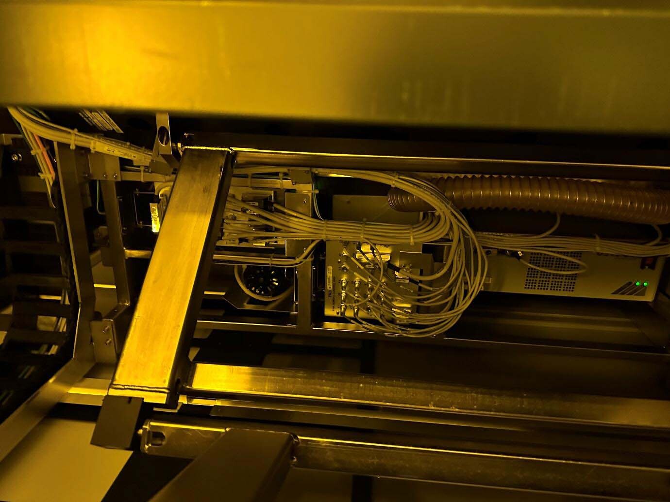
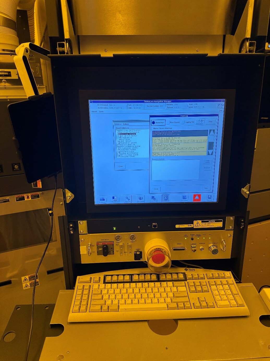
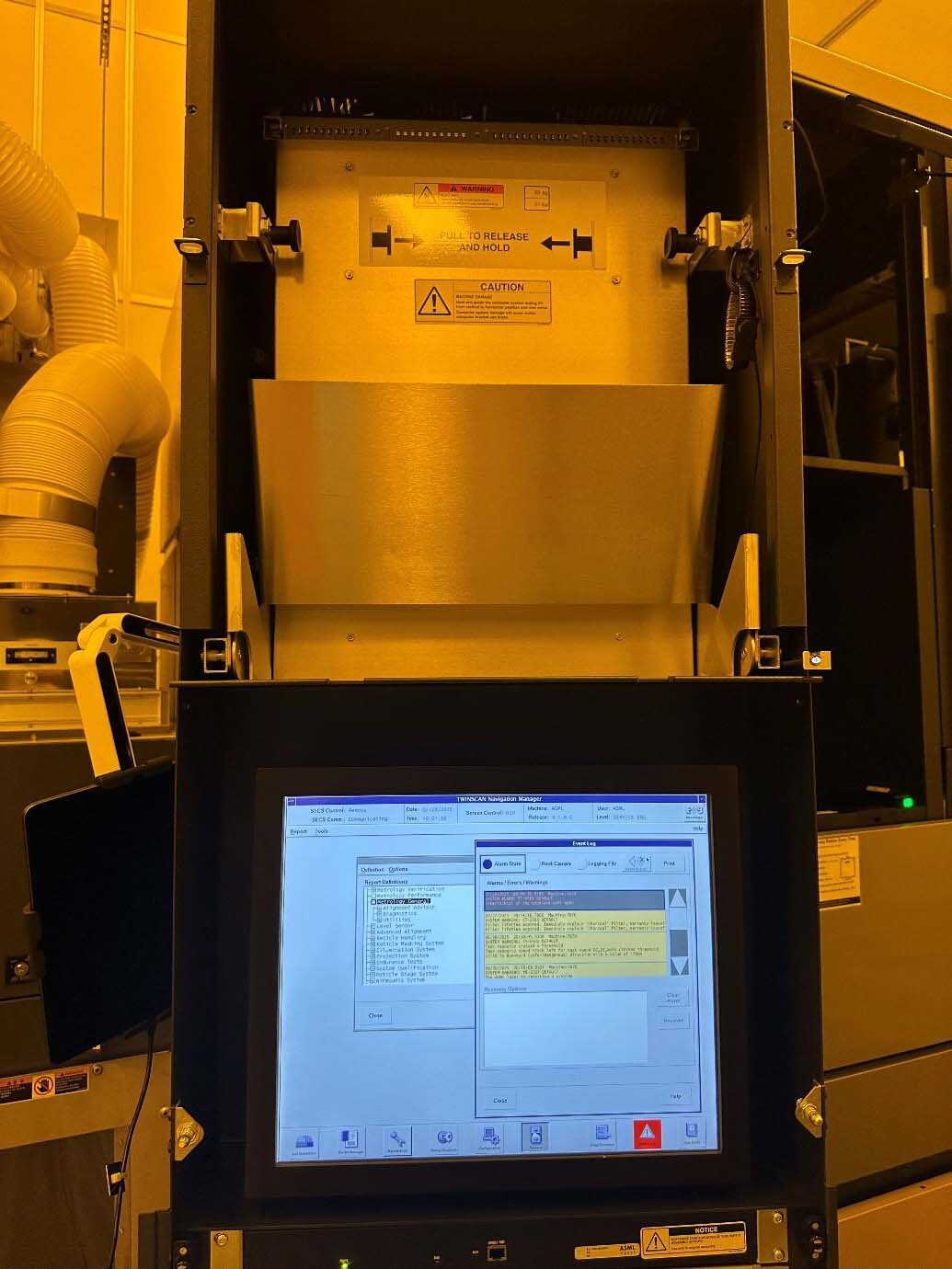
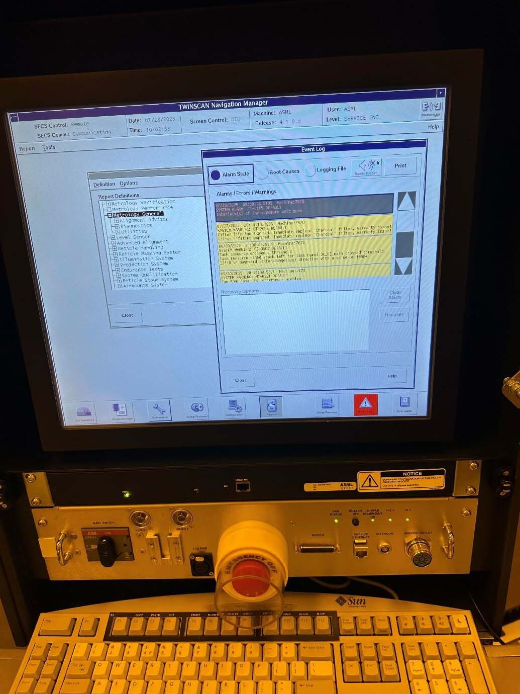
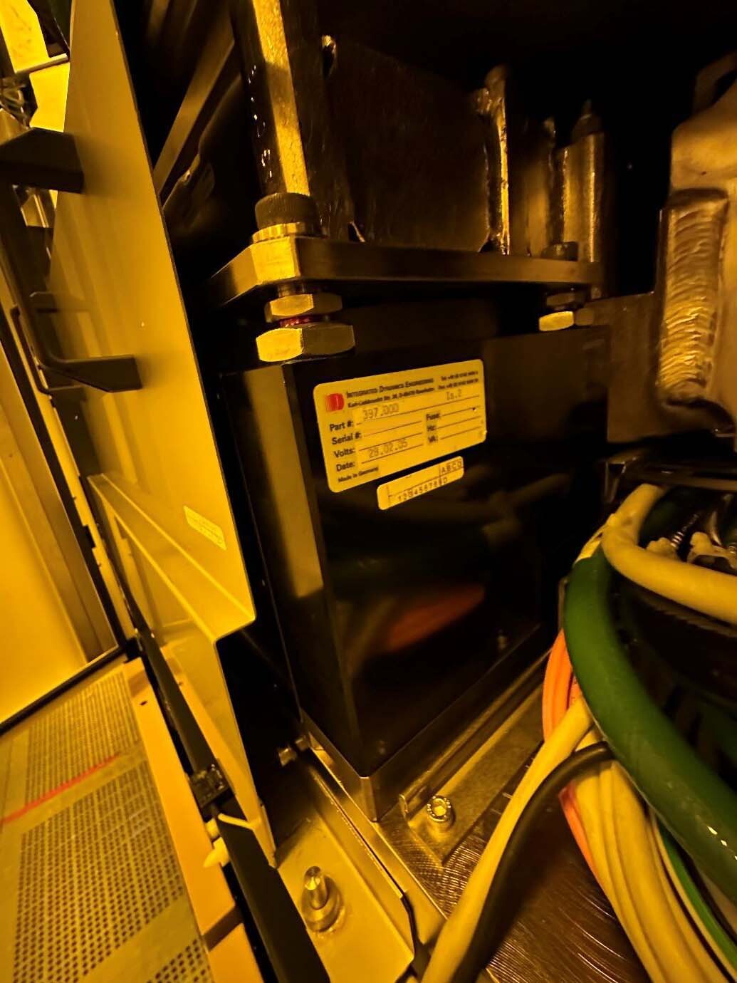
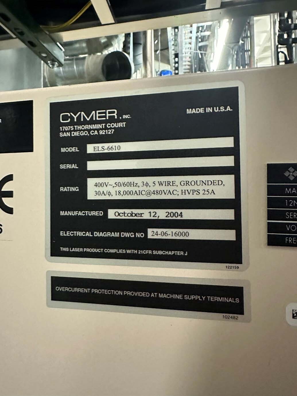
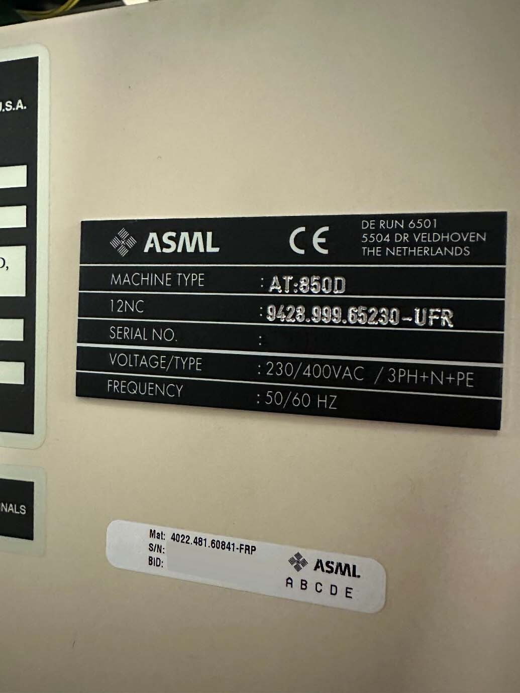
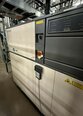
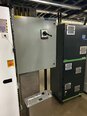
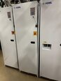
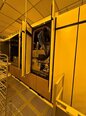
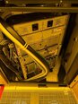
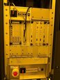
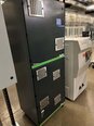
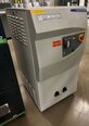
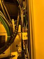
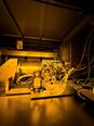
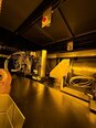
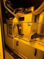
ASML Twinscan AT 850D wafer stepper is a leading-edge, state-of-the-art lithography equipment which offers superior process performance for cost-effective semiconductor wafer fabrication. It is an automated exposure system with step-and-scan capability that enables quick throughput of thin wafers. The unit features high productivity with ultra-fast scan speed and step speed of up to 750 millimeters per second. The AT850D is designed for use in the fabrication of complex, high-density integrated circuits for consumer electronics, computing and memory devices, and low-power applications. The machine contains various advanced optical components, such as quartz lenses, Beam Shaping Optical (5BSO) tool, and an Interference Filter (IF) asset. The optics, combined with advanced lithography software, enable the user to precisely image 6 to 7 levels of circuit components onto the wafer. The AT850D also has a superior scan throughput with advanced thermal compensation technology that significantly reduces the time needed to expose a single circuit layer on a wafer. This reduces patterning-induced distortions on the wafer edge, resulting in finer resolution and higher process yield. The model offers superior accuracy, with micron-level spot to spot accuracy during operations. In addition to its automated scanning capabilities, the AT850D also offers an array of smart features, such as performance diagnosis, calibration, and maintenance monitoring. This enables users to maximize the efficiency of their processes and maintain optimal performance from the equipment at all times. The system comprises of several advanced features, such as a deformable mirror, telecentric lens, AFC Alignment Unit and Data Analysis. These features provide excellent imaging capabilities and allow users to fine tune and calibrate their machine for a variety of applications. Overall, Twinscan AT 850D wafer stepper is an excellent tool for producing complex, high-density integrated circuit components. Its advanced optics, customizable features, and superb throughput make it an ideal choice for semiconductor fabrication.
There are no reviews yet