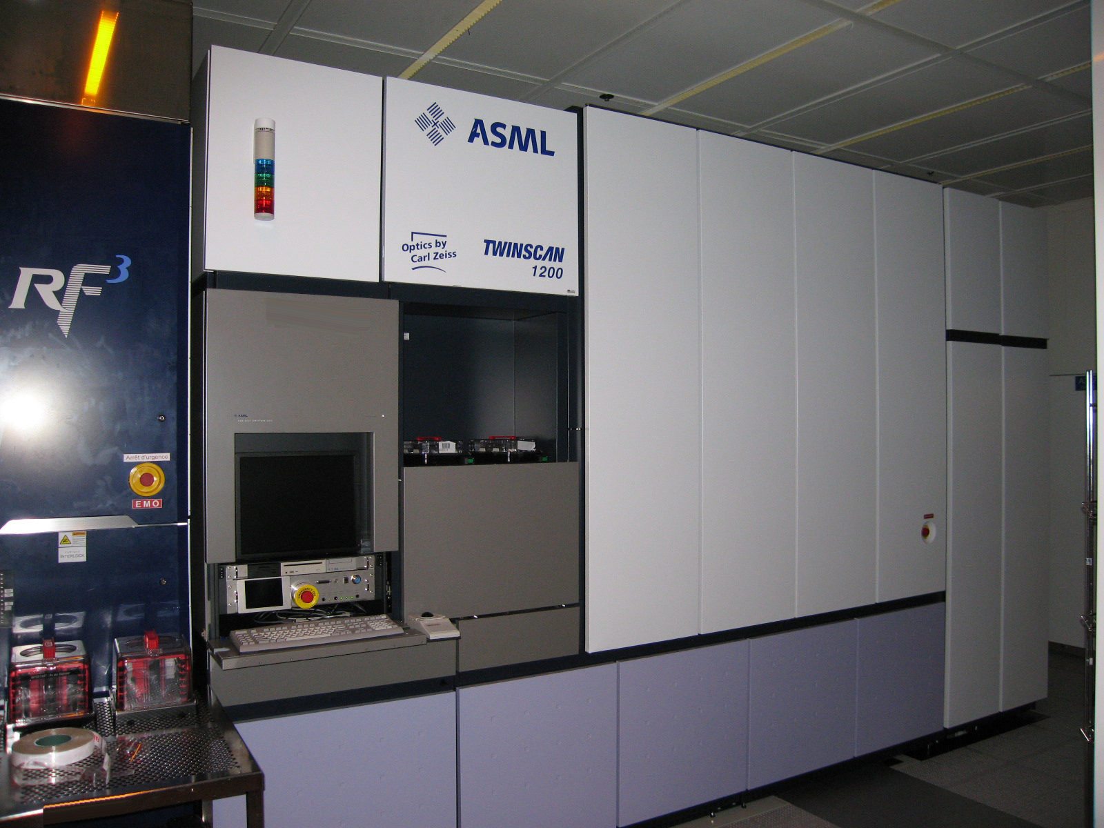
Used ASML Twinscan XT 1200B #9096080 for sale
It looks like this item has already been sold. Check similar products below or contact us and our experienced team will find it for you.
Tap to zoom


Sold
ID: 9096080
Stepper
Slit uniformity: 0.31%
Intensity: 1024.54
Symmetrical error: 0.13%
Max stray light: 0.42%
Slit average: 0.36%
With Unicorn at center: 0.406
SAMOS: 0.89%
Best focus: -0.017
Focus range: 102
AST: 39
Chuck ID 1
Max DX Stdev. DY
1 4.5 2.2 1.8
2 3.5 2.4 0.3
3 3.1 2.1 2.4
4 2.9 3 2
5 2.9 2.1 1
Max DY Stdev. DX
1 3.5 1.6 1.3
2 3.2 1.5 1.6
3 2.9 2 0.8
4 2.8 1.8 2.3
5 2.8 1.6 2.2
Chuck ID 2
Max DX Stdev. DY
1 4.7 4.2 2.8
2 3.7 3.4 2.1
3 3.4 4.3 0.2
4 3.2 3.9 3.2
5 2.7 4.2 0.7
Max DY Stdev. DX
1 3.6 2.9 0.7
2 3.5 1.9 0.9
3 3.4 2.3 0.2
4 3.2 2.9 3.2
5 2.8 2.3 2.3
342/440 VAC, 48/52 Hz, 30 kVA.
ASML Twinscan XT 1200B is an advanced wafer stepper for the manufacture of integrated circuits. It is used to accurately pattern photomasks onto semiconductor wafers during chip fabrication. The XT 1200B is based on ASML twin-beam scanning technology and features a state-of-the-art optical sub-system and a high- performance scan field effectiveness. The XT 1200B is equipped with two diffractive optical elements (DOEs) in each projection unit and includes an integrated resist imaging system. The DOEs employ two separate optical paths to precisely correct for aberrations in order to produce focused sub-micron line patterns. The integrated resist imaging system provides a low-copy masking of thin or thick layers of patterned photoresists. The alignment accuracy of the XT 1200B is 12nm (1σ) with 2nm of drift, improving the etch and yield of the finished product. It implements the measurement and monitoring of critical machine parameters such as reticle/wafer flatness, beam uniformity, positioning and pointing accuracy, and even electrical behavior of the substrate during patterning. The XT 1200B boasts a reticle scan field of 12 inches, a full field scan rate of 15.25 million pixels per second and a total wafer scan rate of 124 million pixels per second. Its maximum numerical aperture of 0.25 provides a resolution limit of less than 0.25 micrometer. The XT 1200B also features large doses of up to 600mJ/cm^2 that enable faster exposures in the case of thicker resists. In addition, this model offers a full suite of data analysis and reporting tools that allow users to optimize the machine performance with respect to resist imaging, overlay, and lens damage. The XT 1200B also comes with automated stage calibration and aberration correction for continued stability and performance. All in all, Twinscan XT 1200B is a state-of-the-art wafer stepper that is well-suited for high-volume production of advanced semiconductor devices. It combines excellent alignment accuracy, high throughput, and advanced features such as aberration correction and integrated resist imaging to make sure that every batch of semiconductors comes out of the factory perfect.
There are no reviews yet