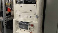
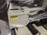
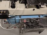
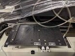
Used GCA DSW 8000 #9312611 for sale
URL successfully copied!
Tap to zoom
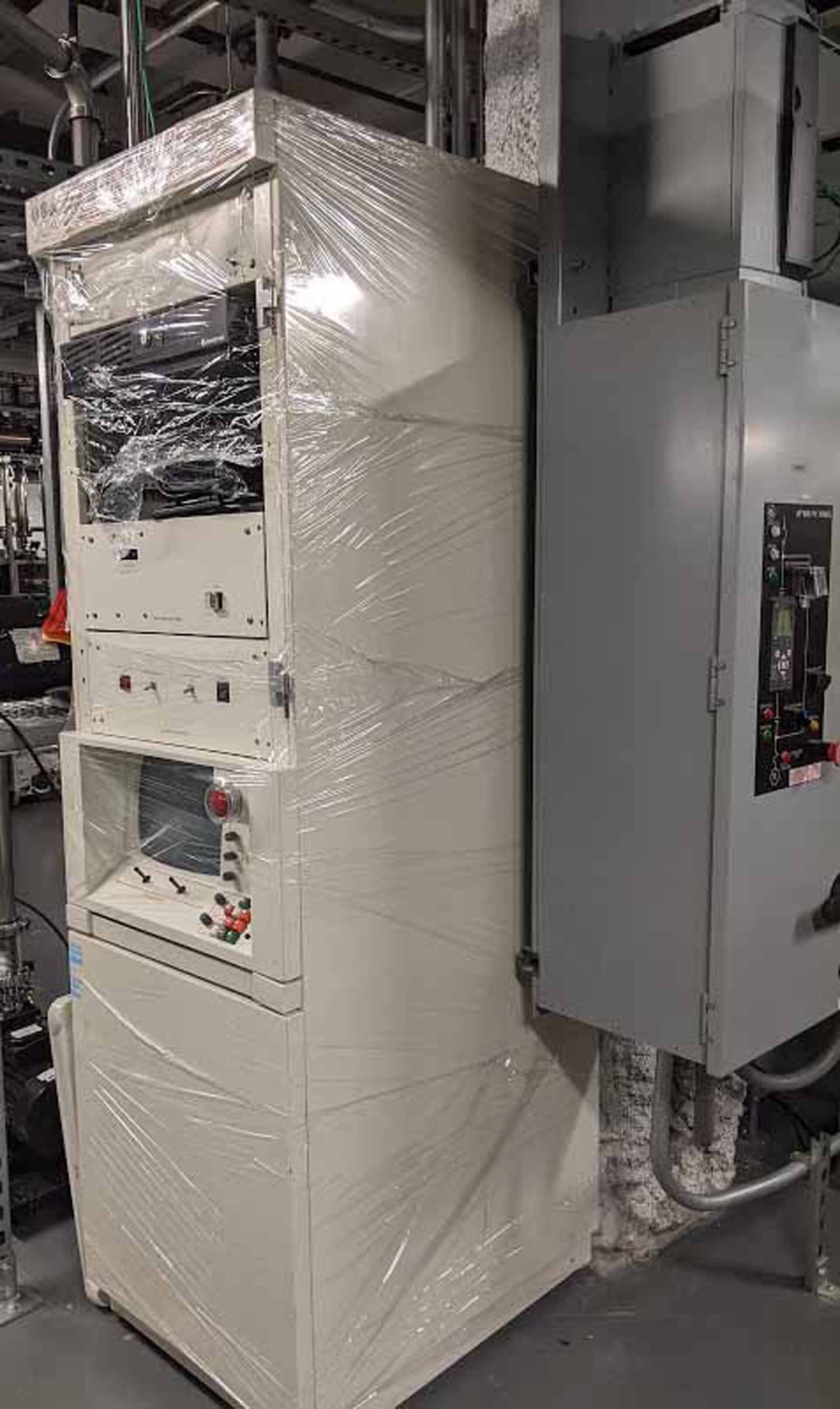

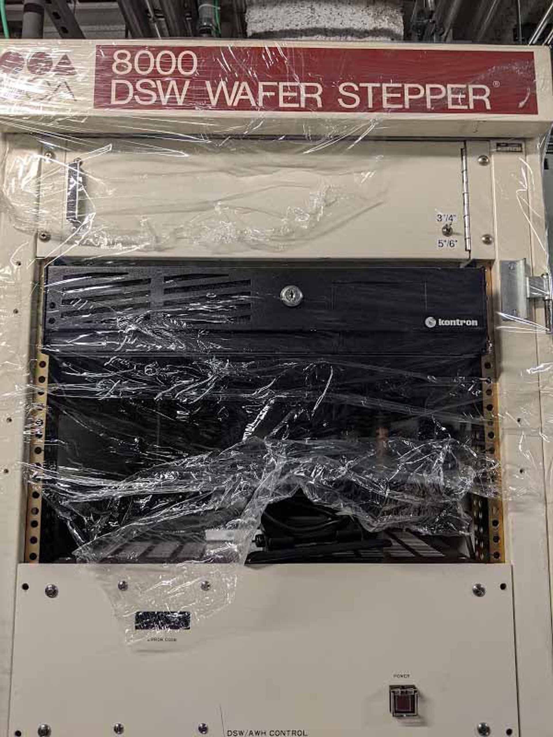

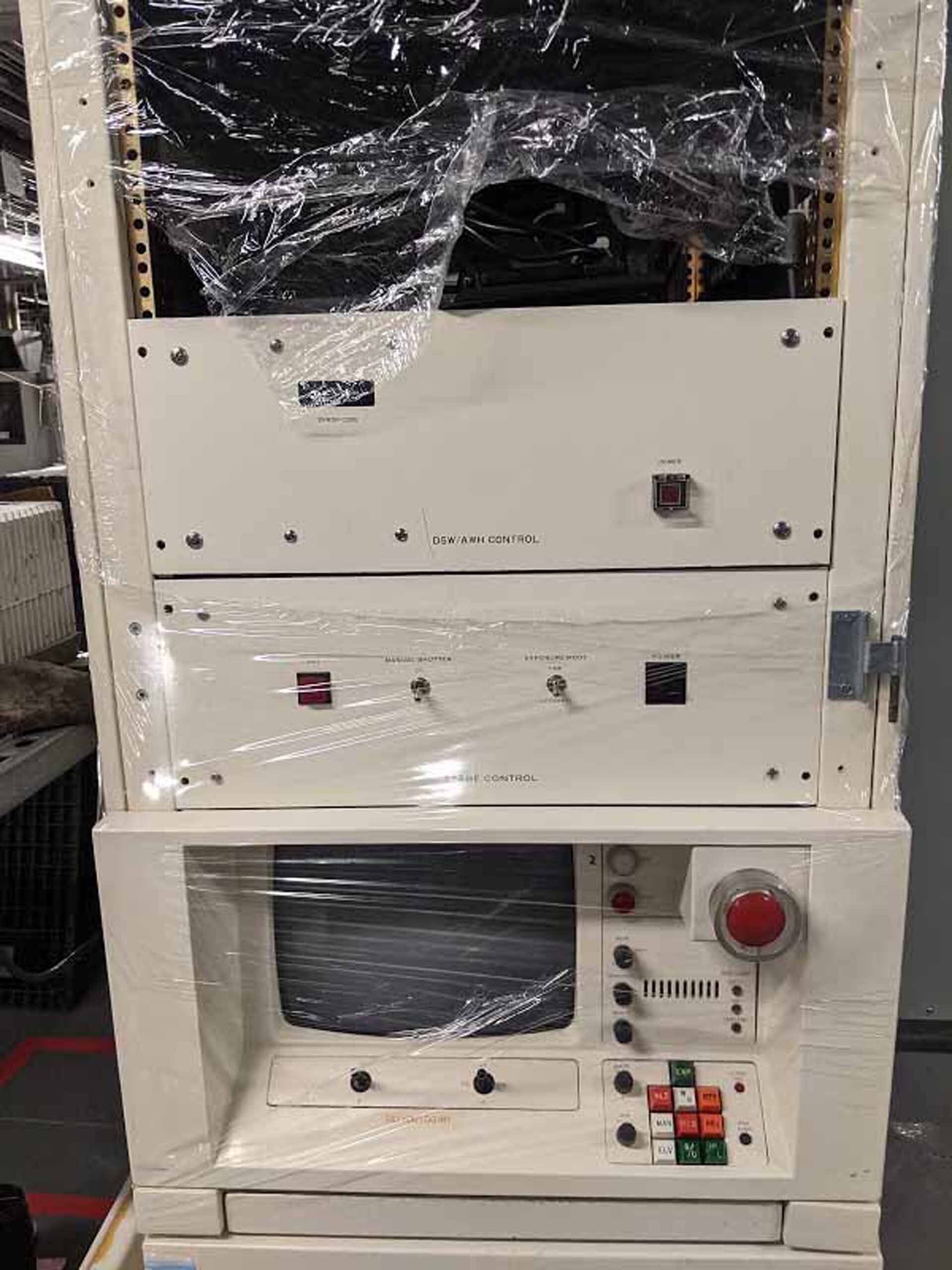


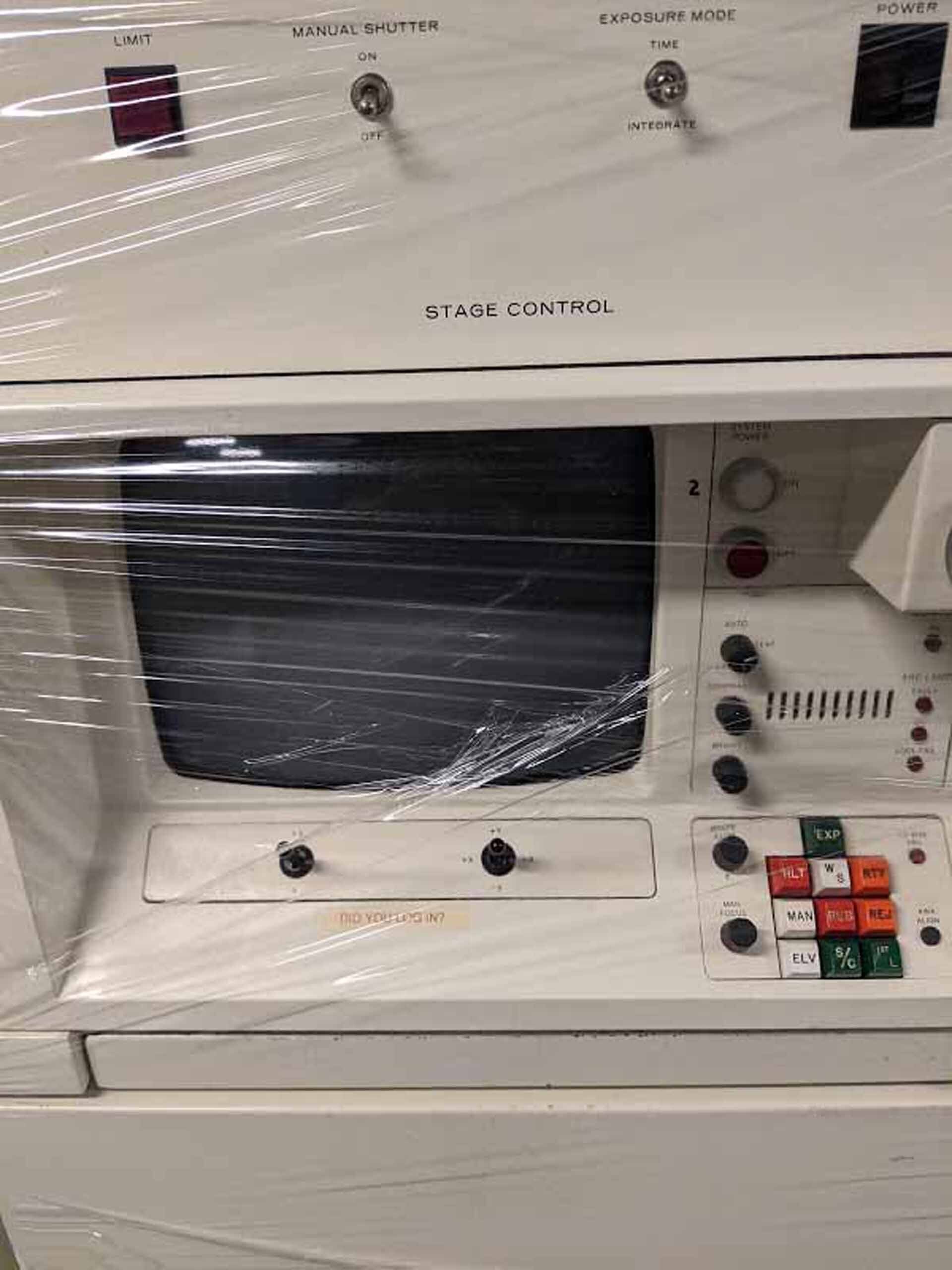

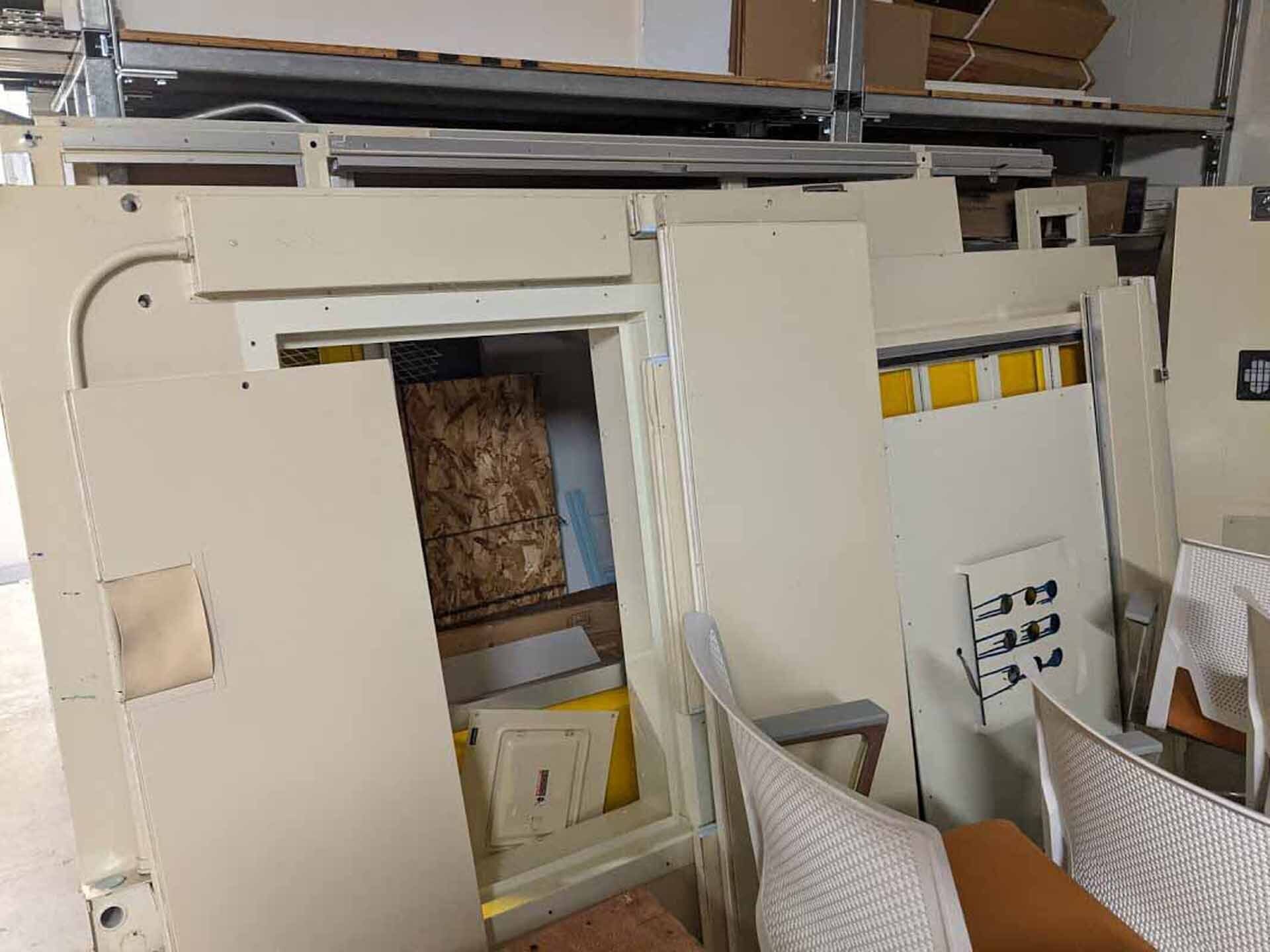

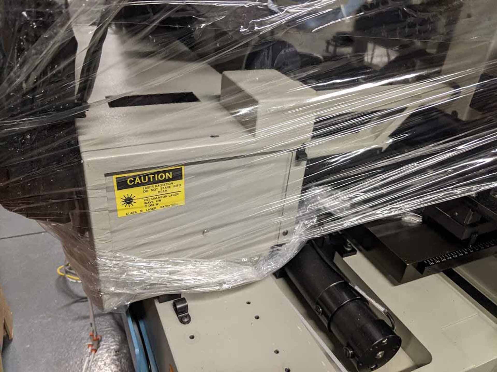

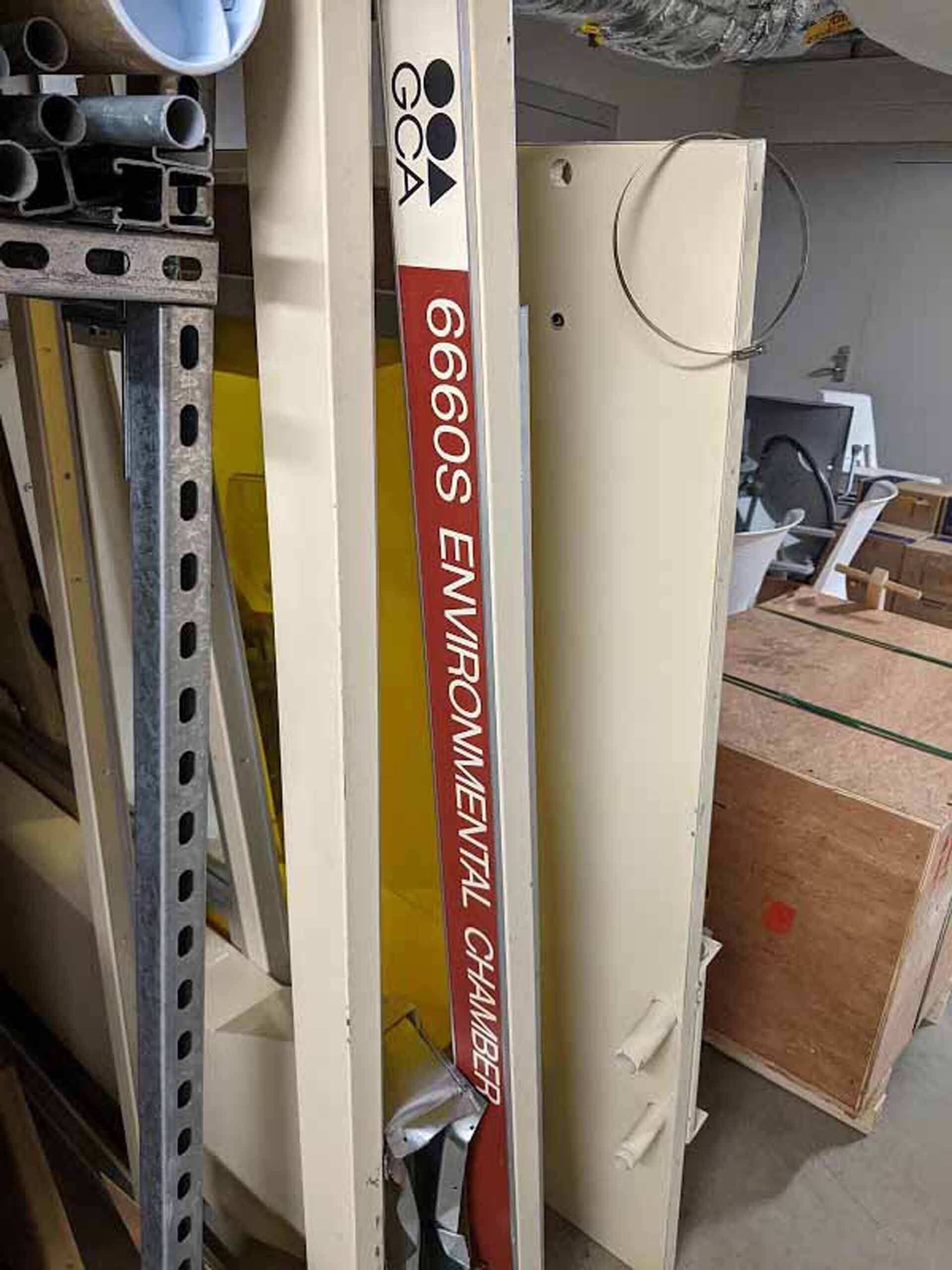

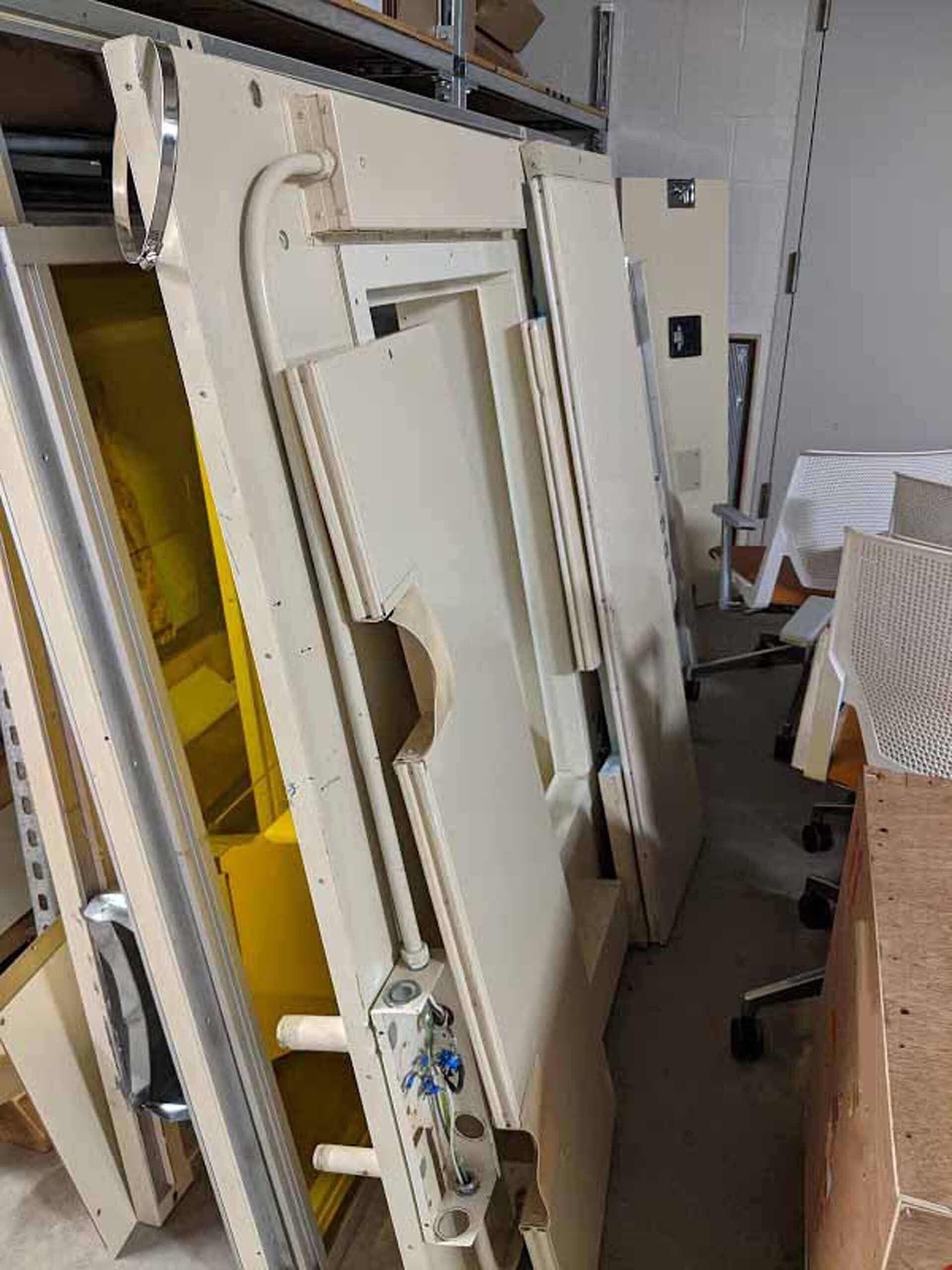

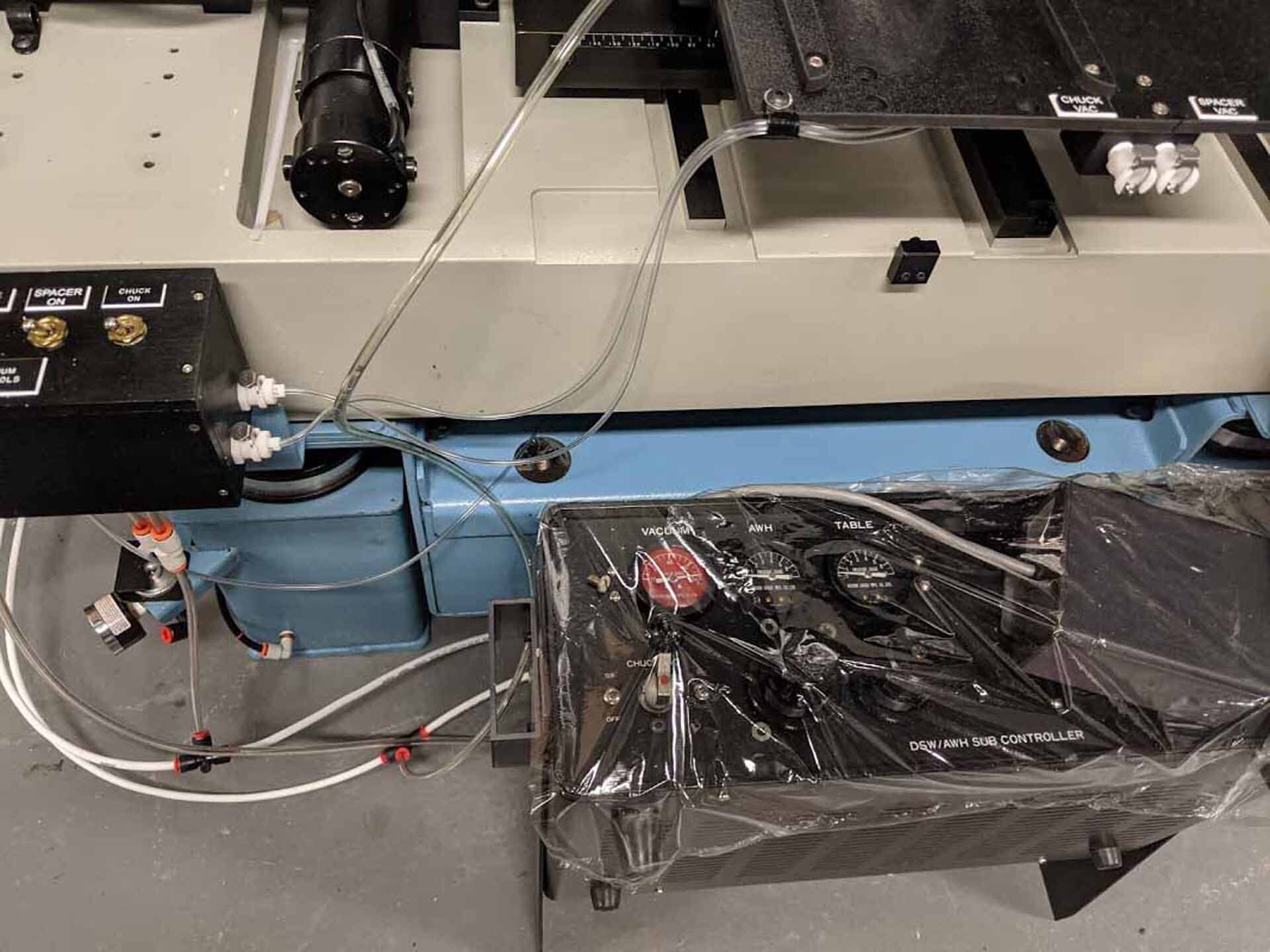


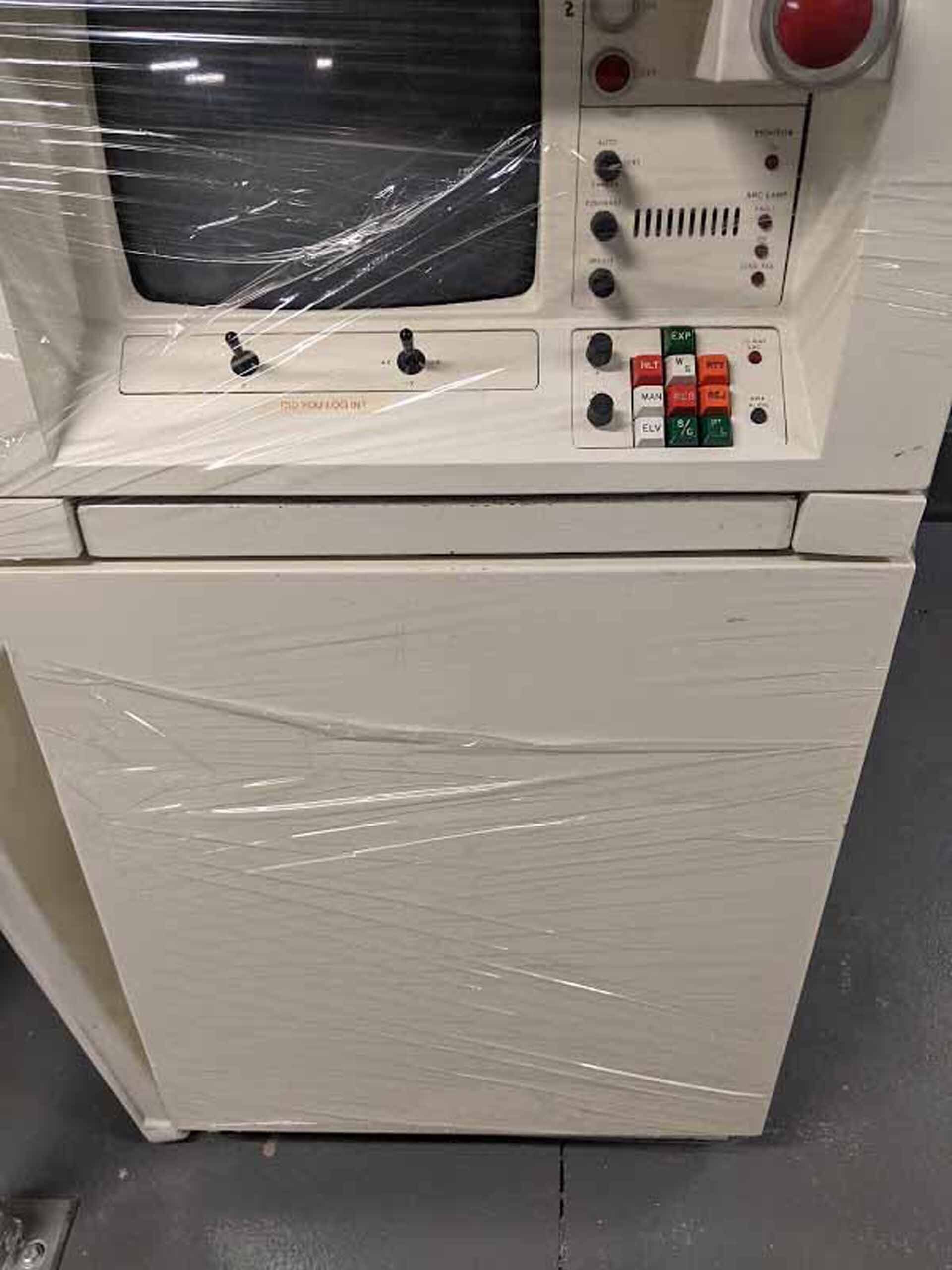

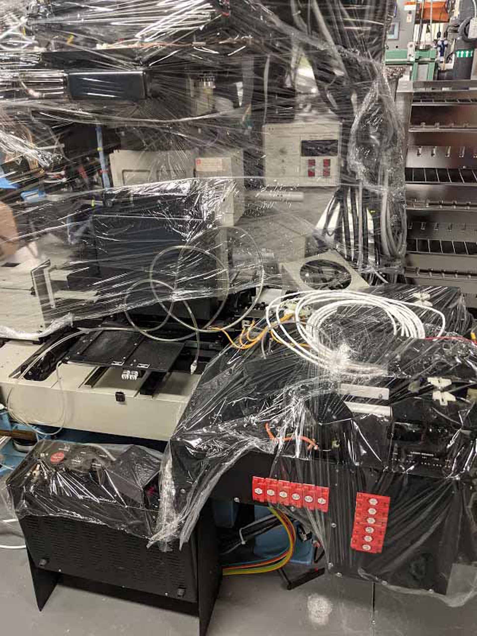

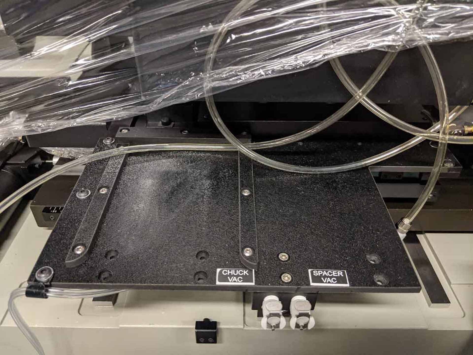




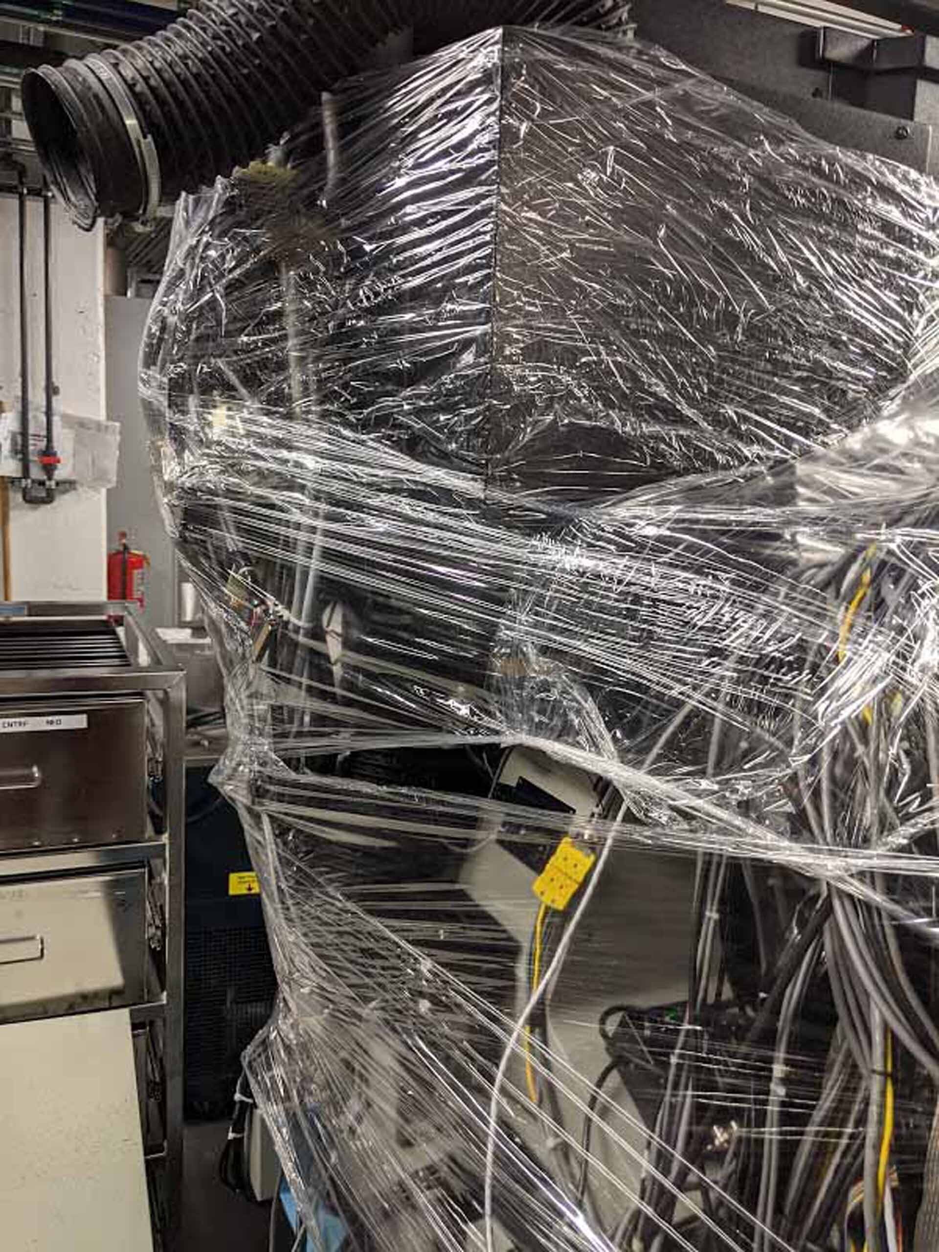

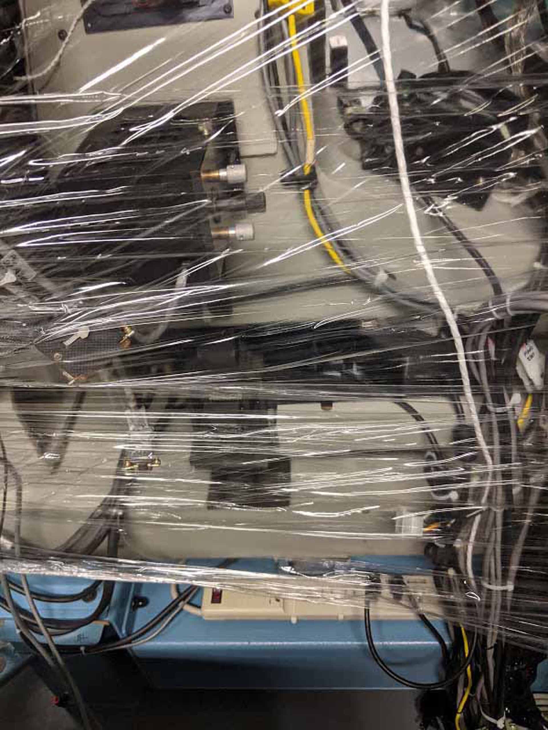

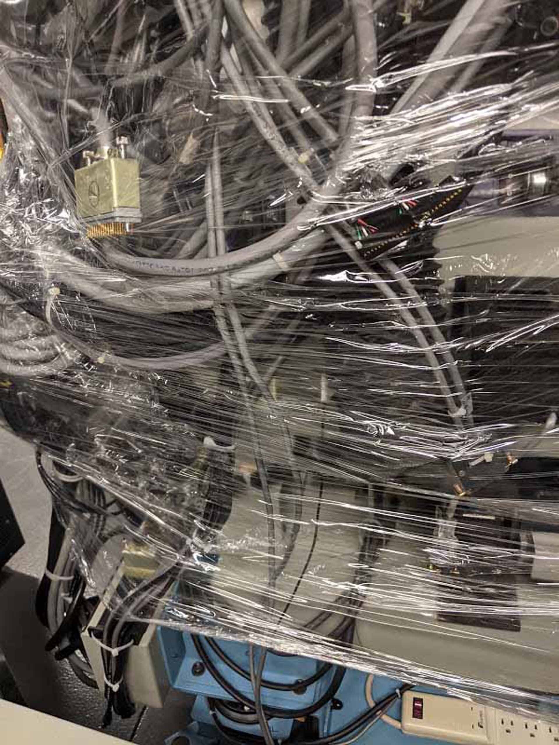

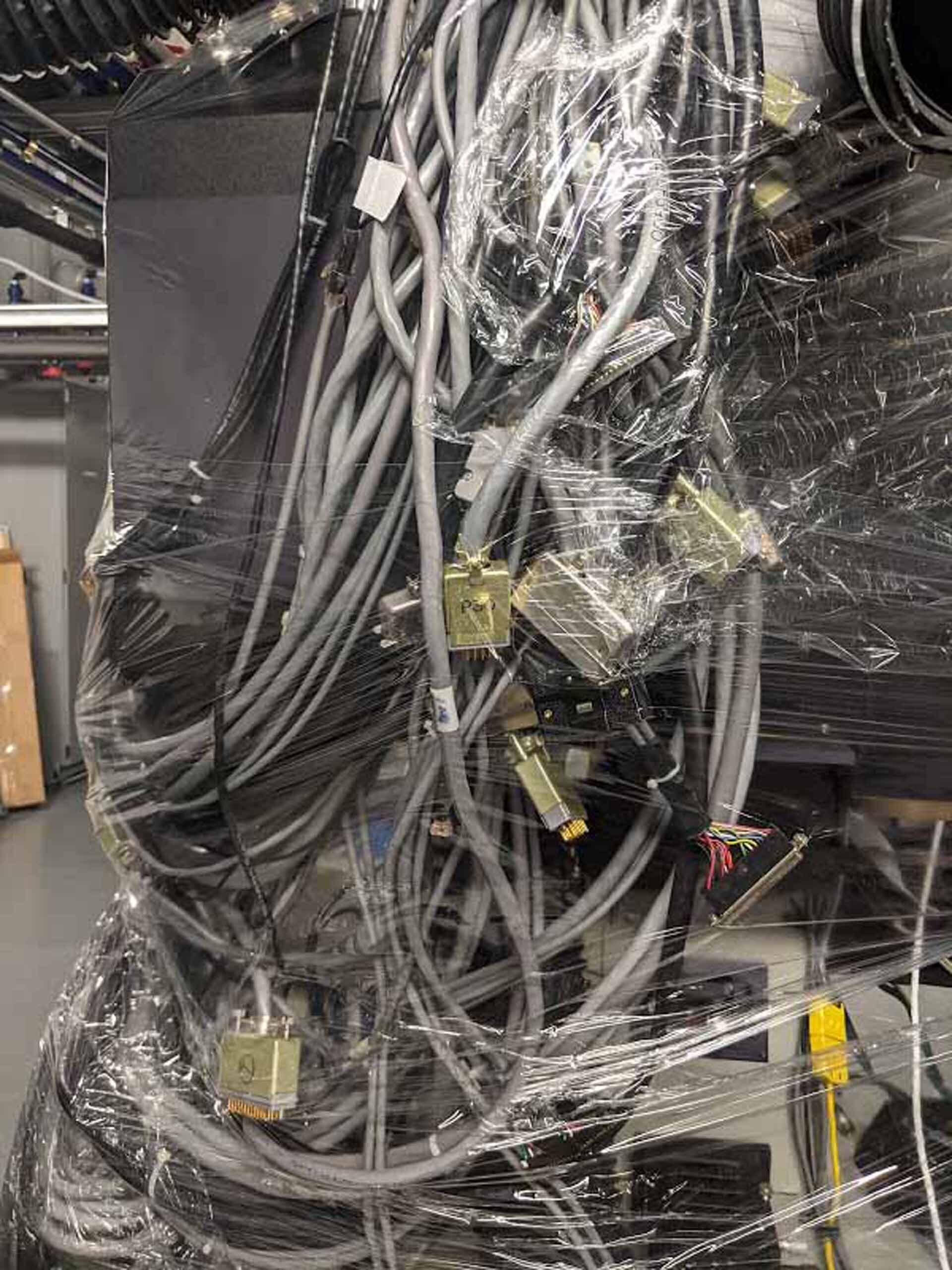


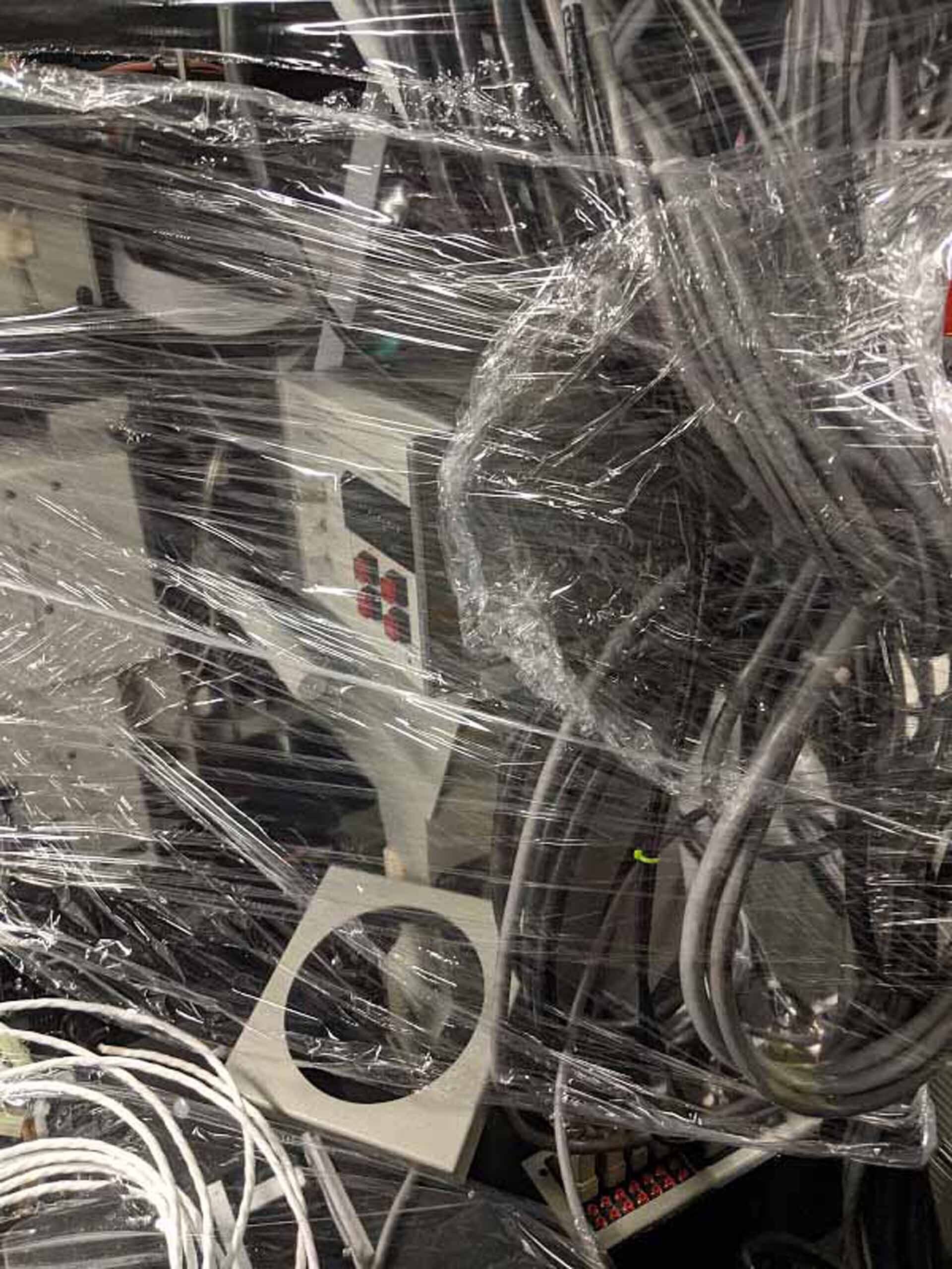

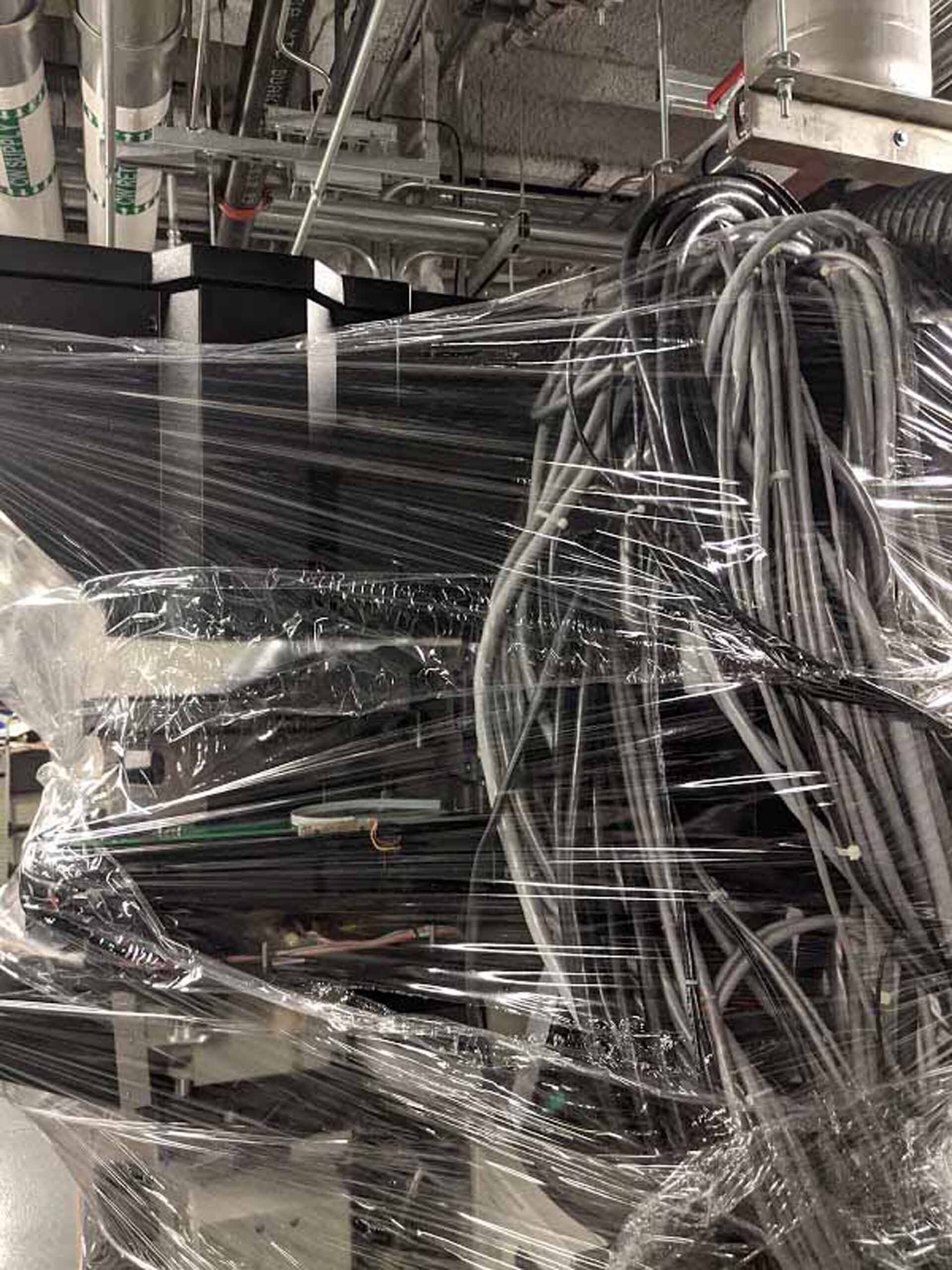

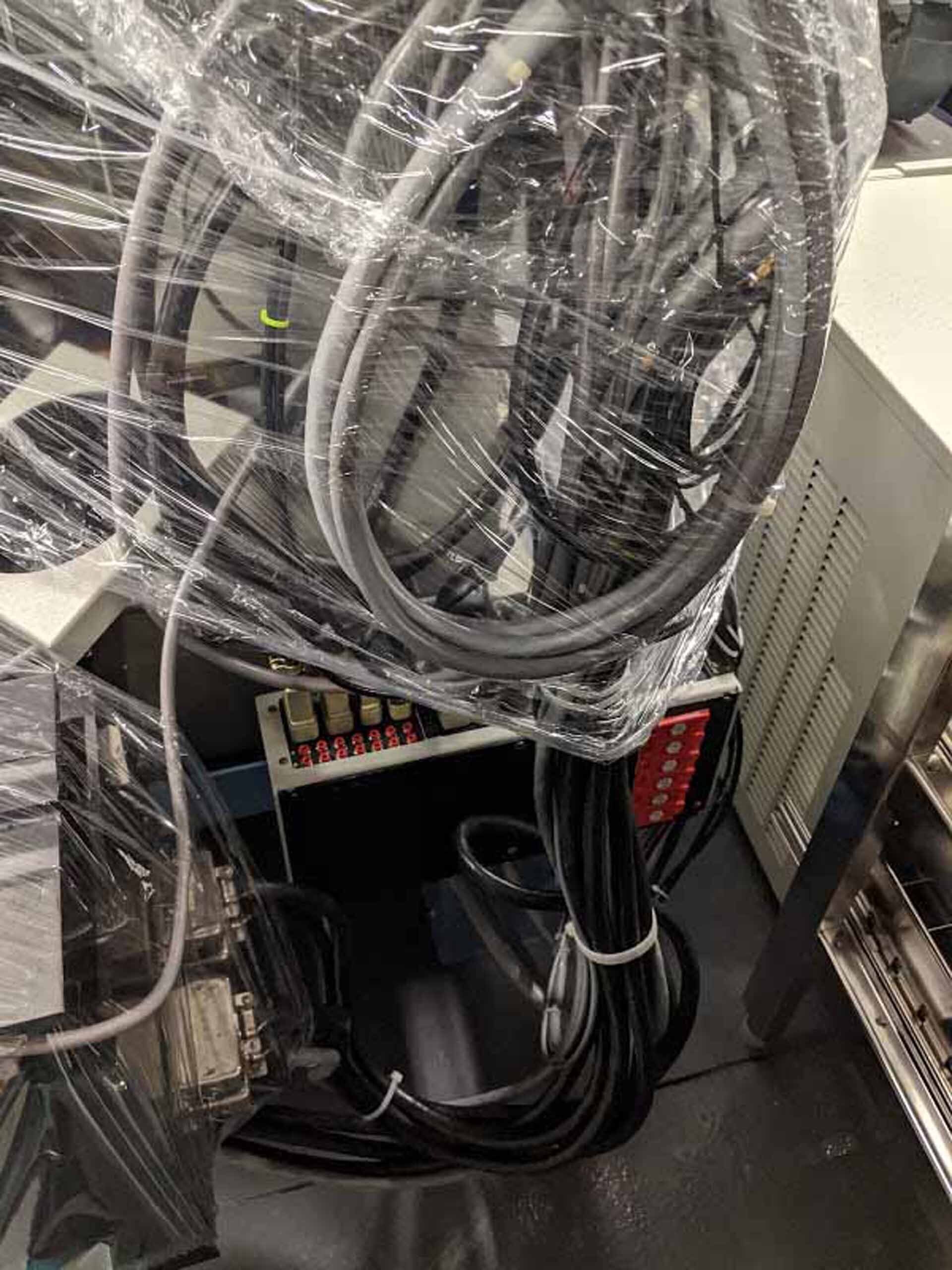


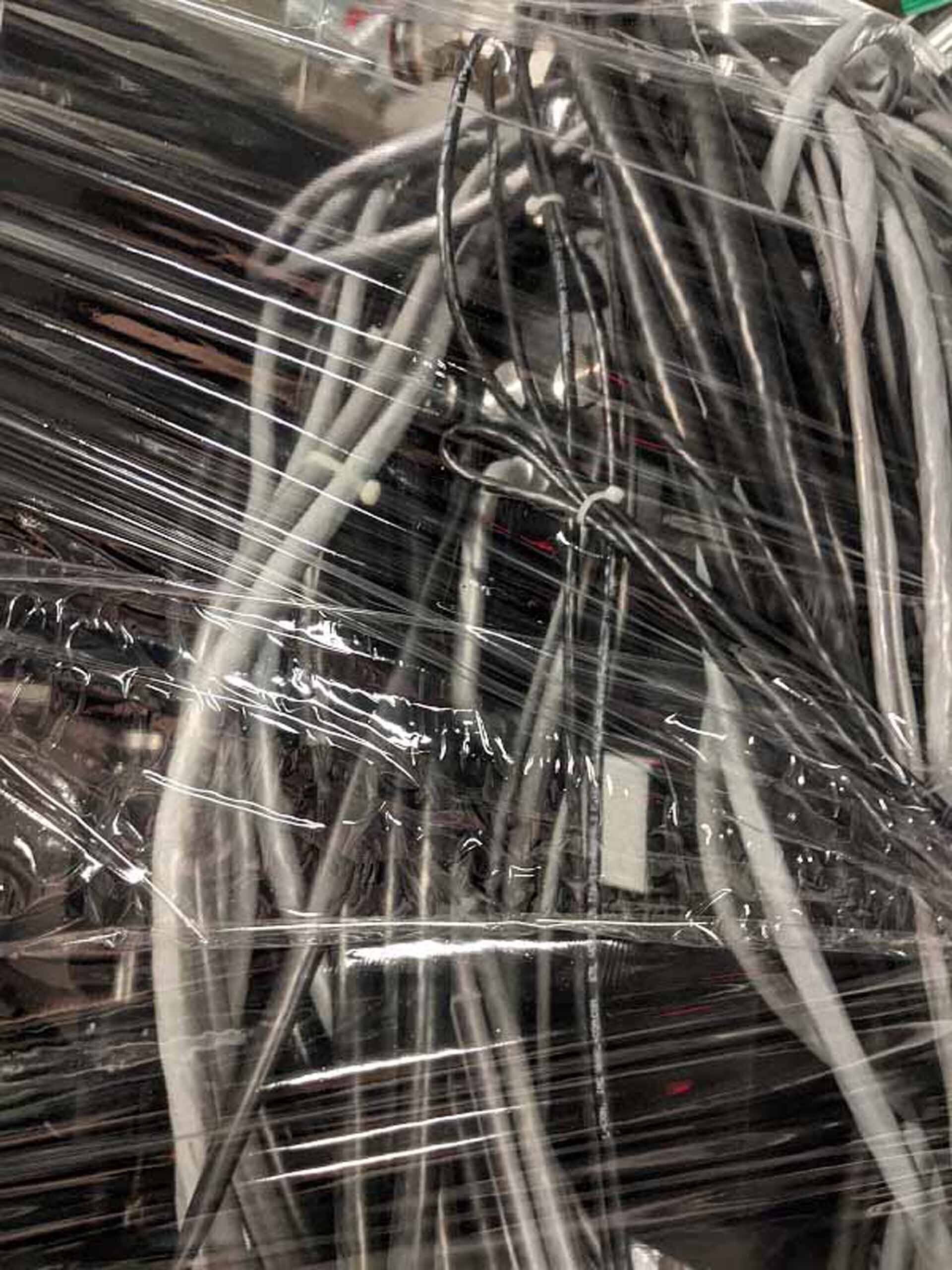

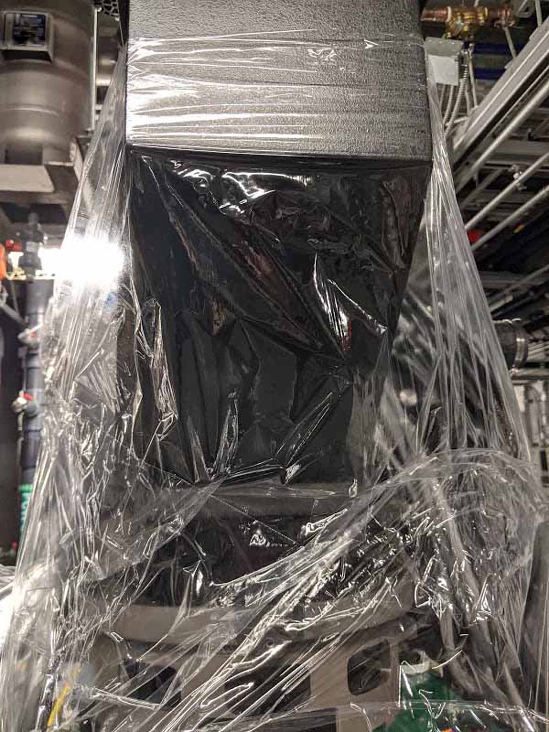

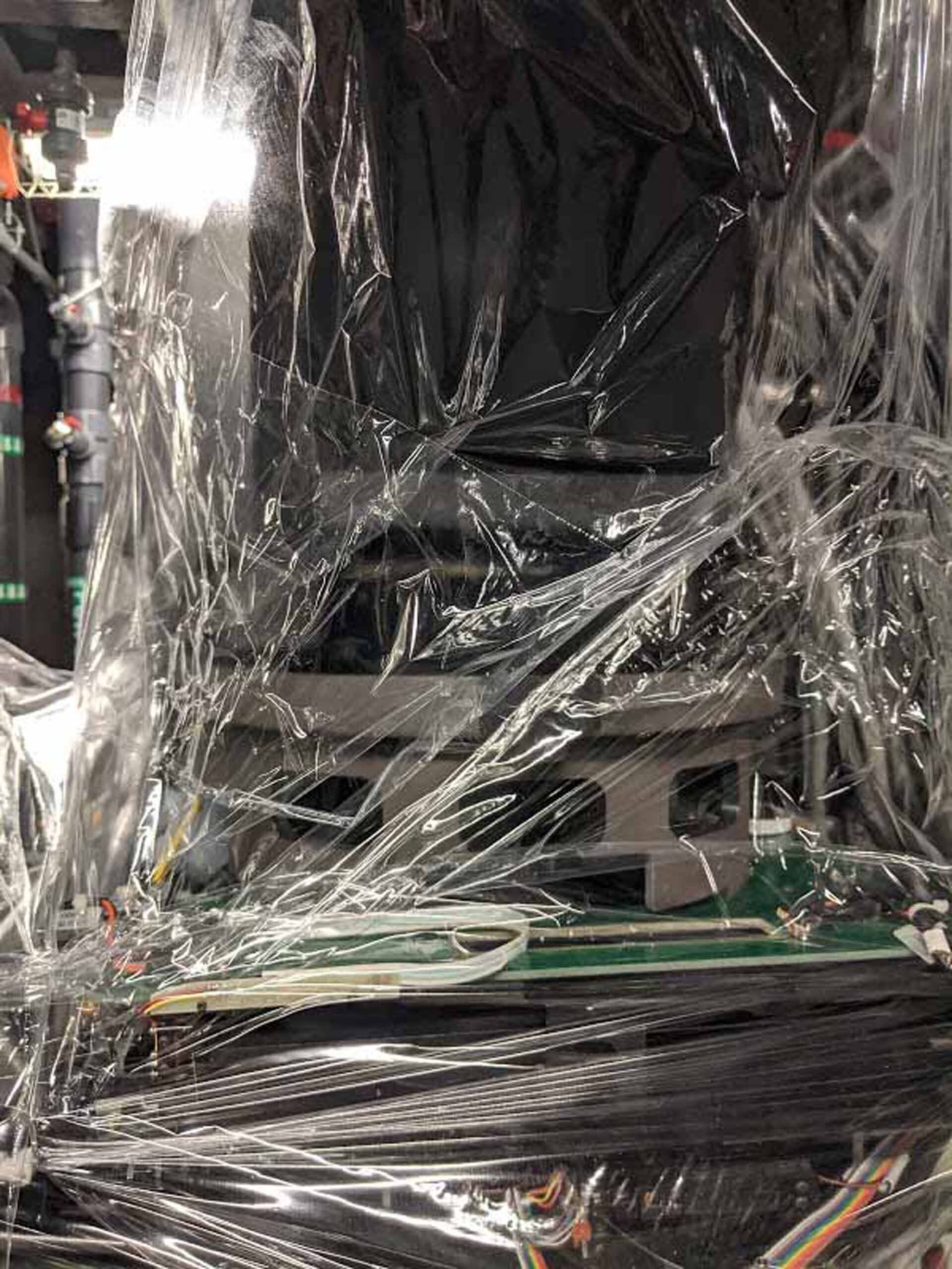

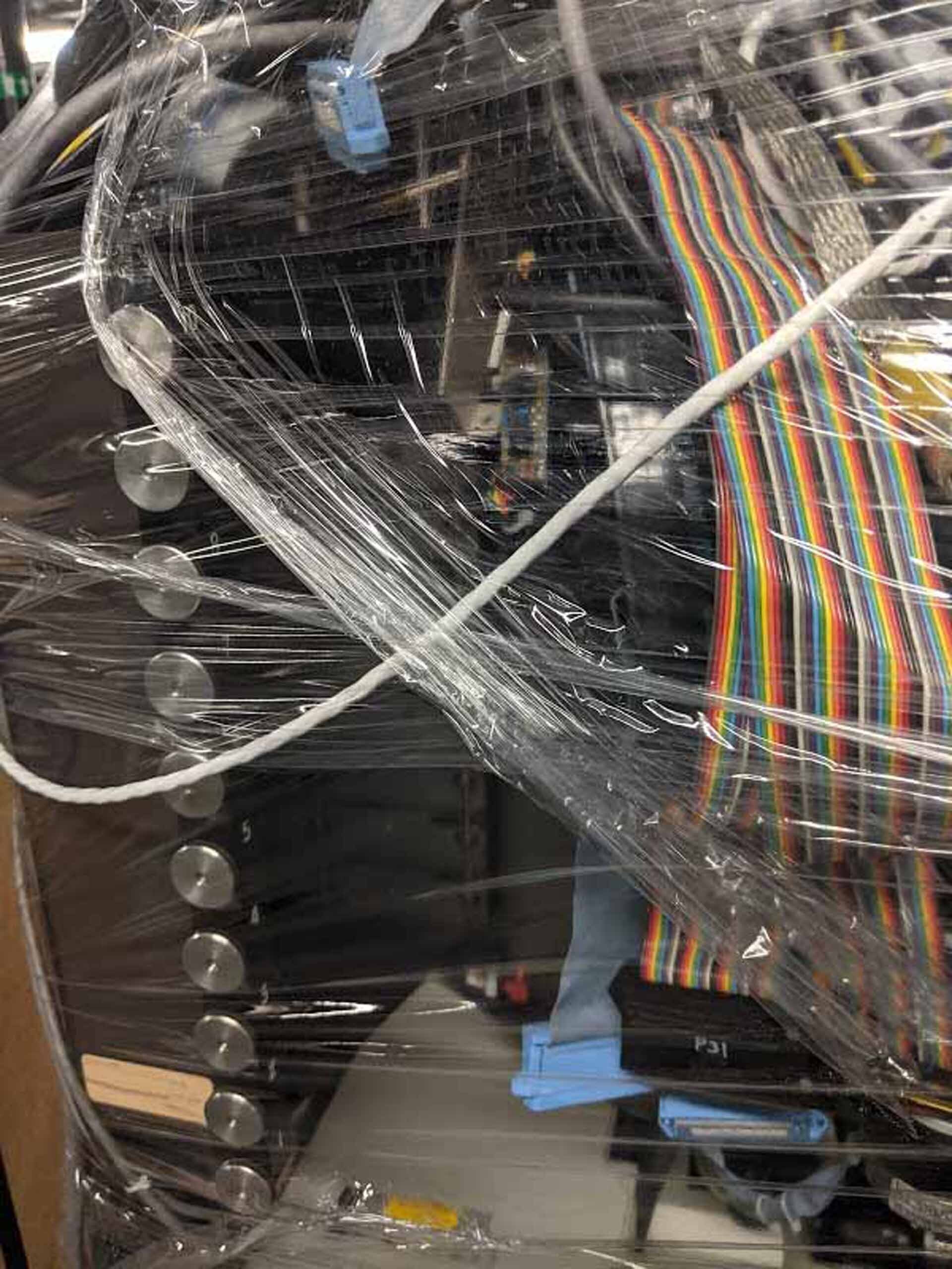

GCA DSW 8000 is a highly advanced wafer stepper used in the semiconductor manufacturing industry. It is an automated equipment that exposes patterned images onto silicon wafers for use in integrated circuit devices. This device utilizes an advanced binary optics technology to achieve unparalleled speed and accuracy in exposing the patterned images. It is equipped with an 8-0 inch step size, which enables it to accurately project images onto wafers as small as eight microns. In addition, the system boasts a resolution of 0.25 micron, giving it exceptional levels of detail and accuracy. DSW 8000 is capable of handling both selected area imaging and aerial image projection, providing users with the ability to adjust image size and shape as needed. Additionally, the device includes an automated alignment unit for accurately positioning each individual image on the wafer. An integrated anti-reflective coating machine helps achieve optimal levels of exposure quality, resulting in a sharper, brighter image. The tool also comes with Real-Time Process Monitoring, which allows users to easily monitor and troubleshoot any issues that may arise during exposure. In terms of safety, GCA DSW 8000 is equipped with a variety of protective layers and technologies to prevent any radiation exposure to users. This includes a unique shutter asset that covers the exposure area, ensuring that no radiation enters the chamber. The device is also designed to reduce the production of static electricity, helping to prevent the introduction of any foreign material into the imaging chamber. Overall, DSW 8000 is a versatile, highly advanced wafer stepper designed to provide users with exceptional speed and accuracy when imaging silicon wafers. It features a variety of safety features and technologies to help ensure maximum user and image protection, while its automated alignment and anti-reflective coating systems help improve the clarity and brightness of the images. The device's 8-0 inch step size also provides unprecedented levels of detail and resolution, making it an ideal choice for semiconductor manufacturing operations.
There are no reviews yet


