Used HITACHI LD-5011iA #9085774 for sale
URL successfully copied!
Tap to zoom
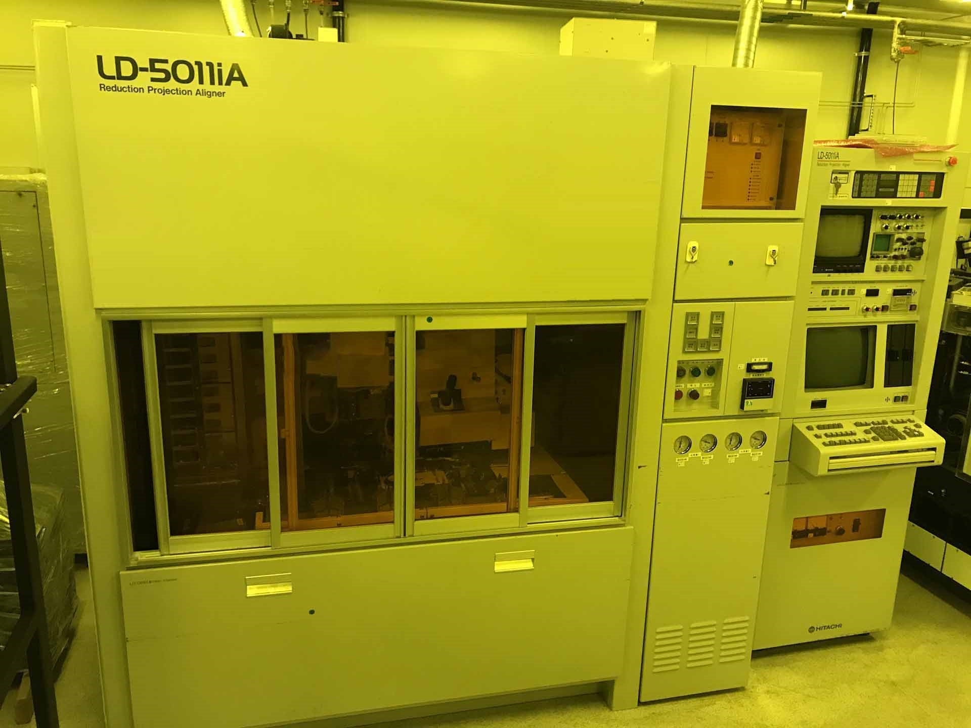

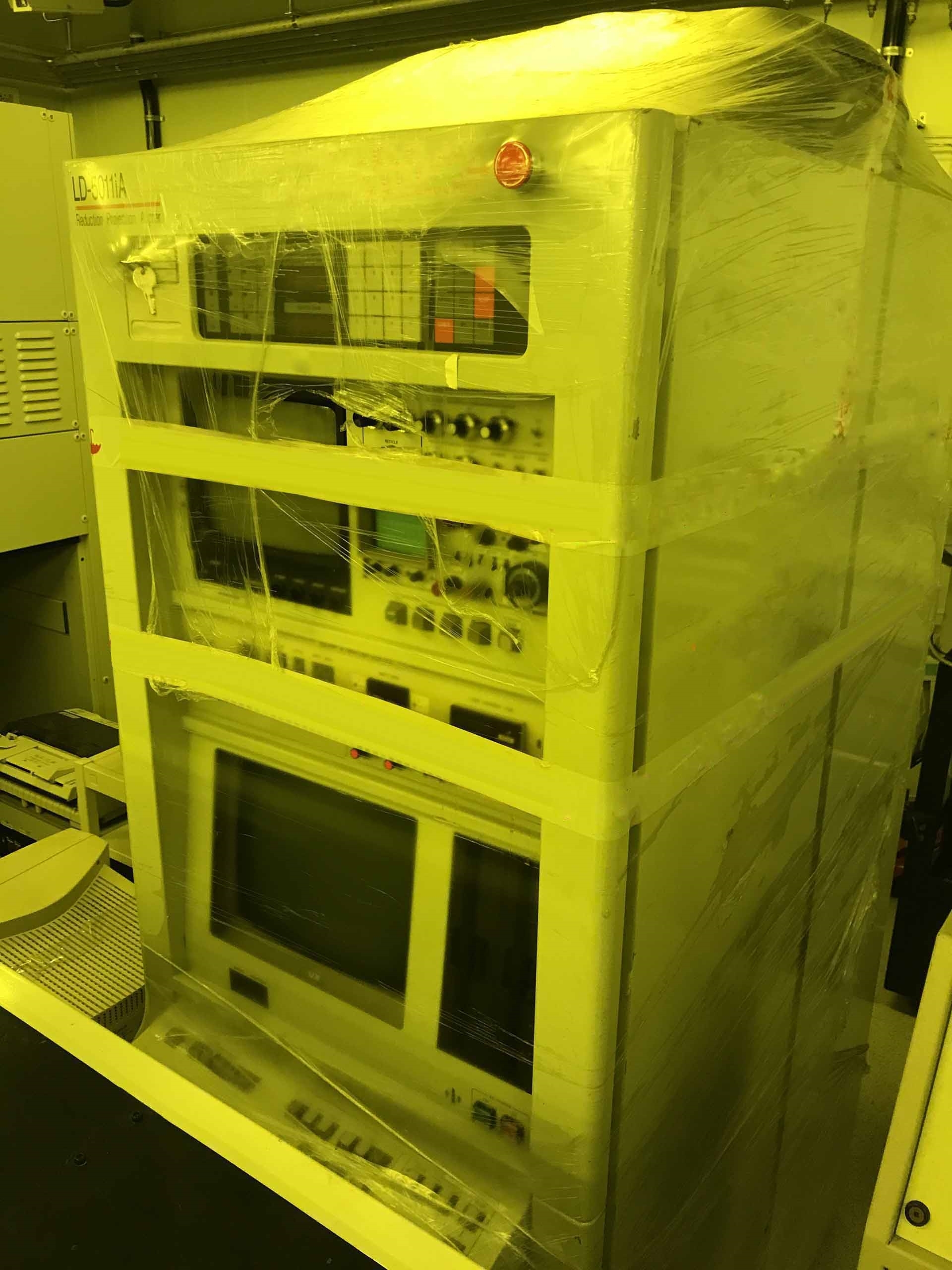

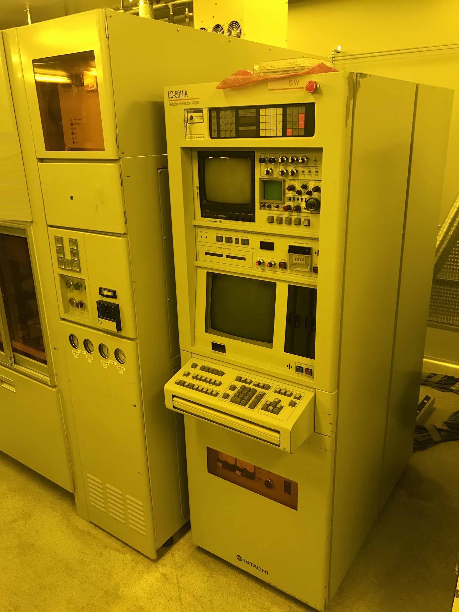

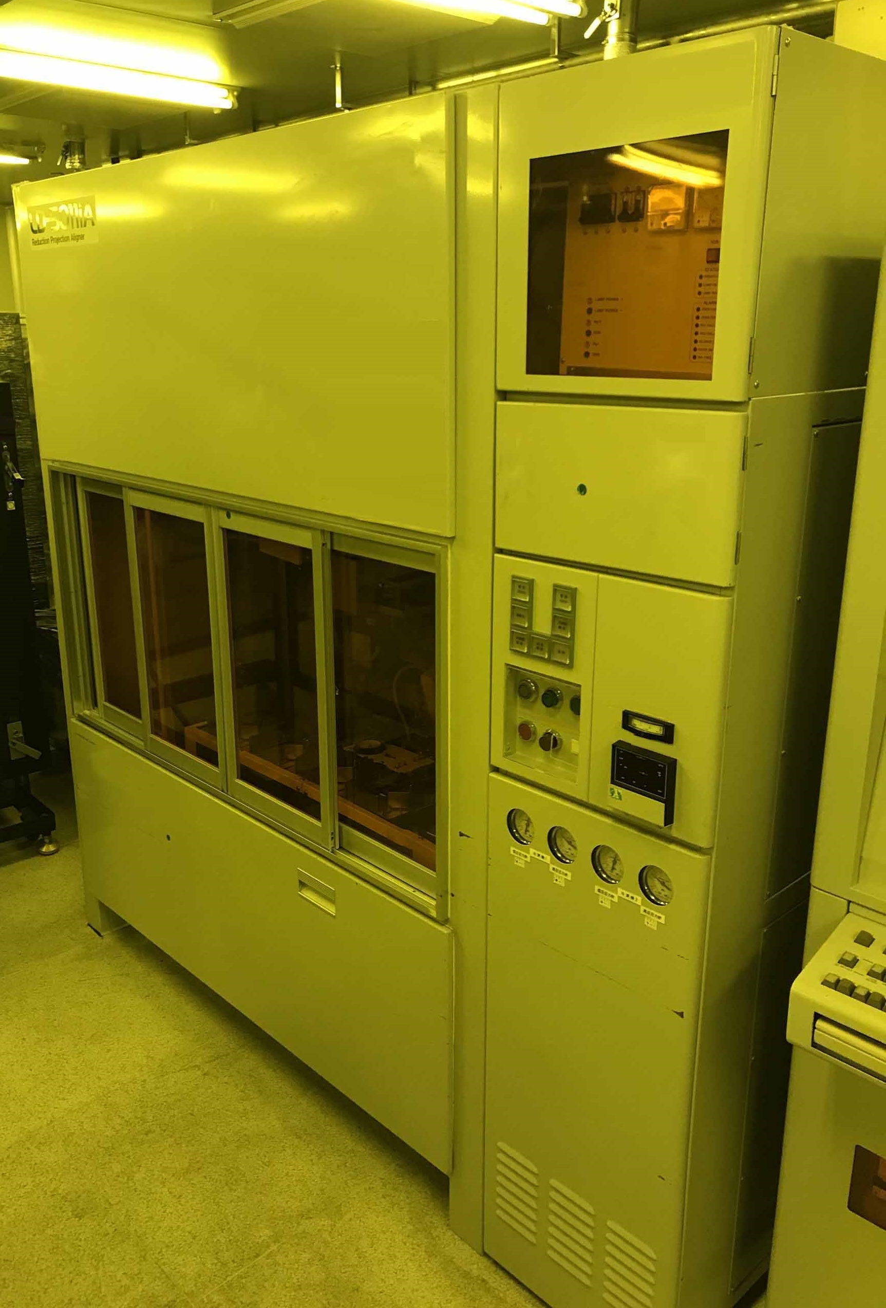


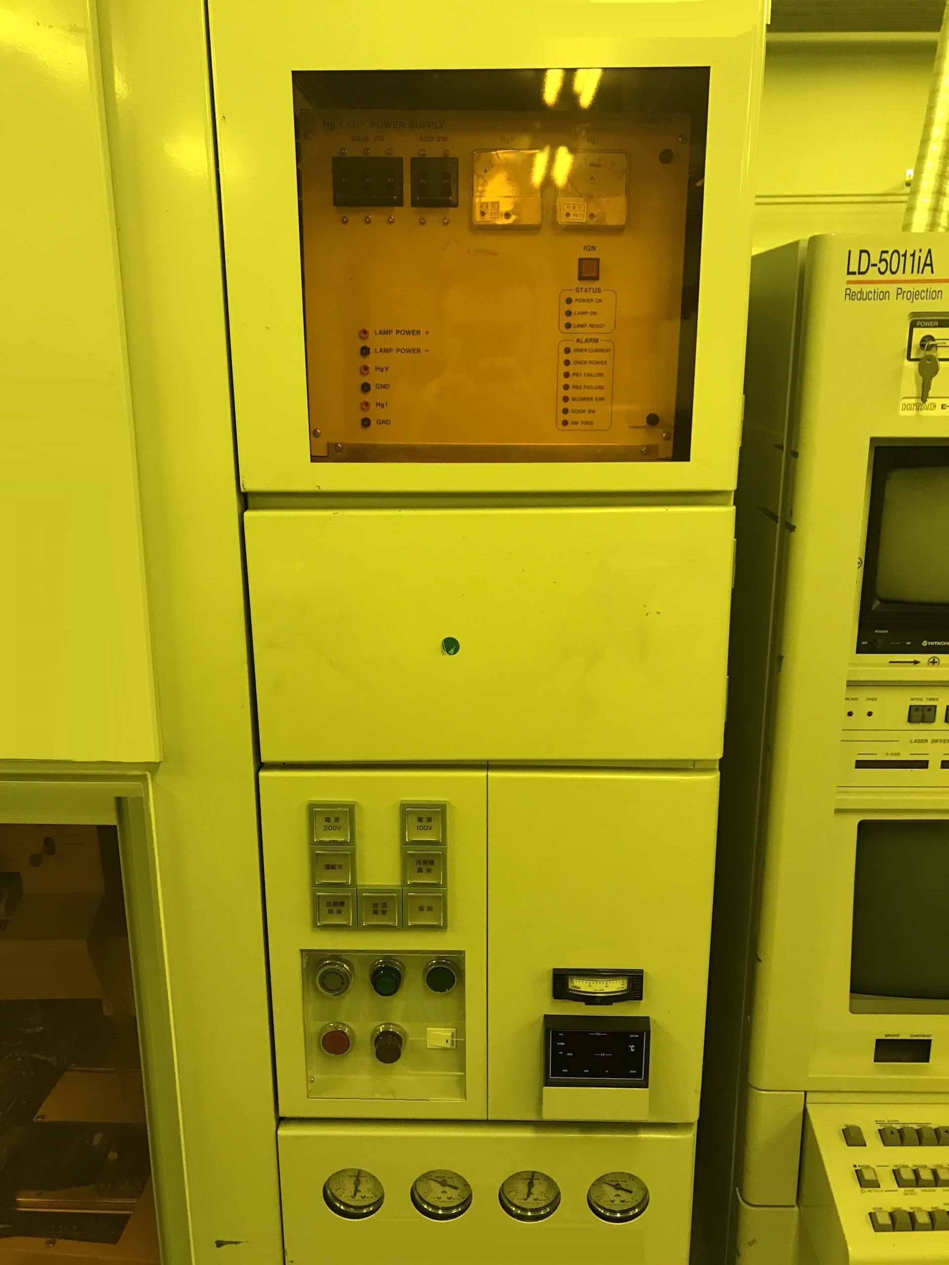

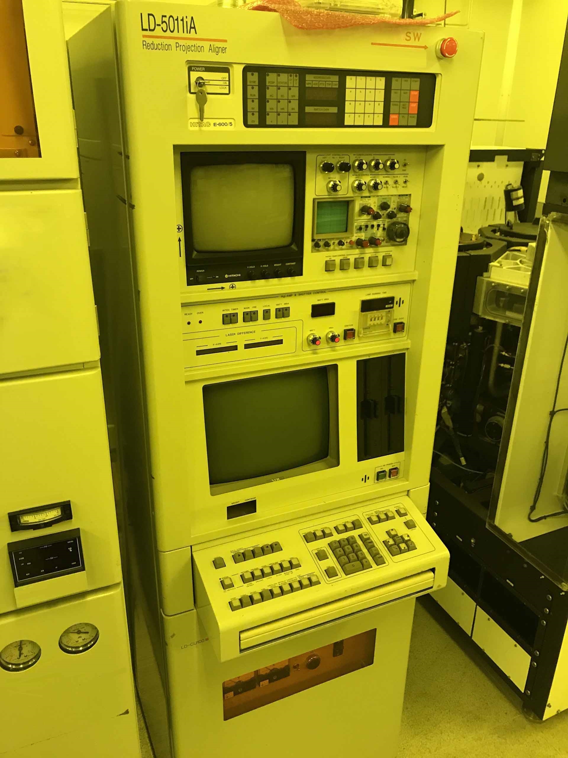

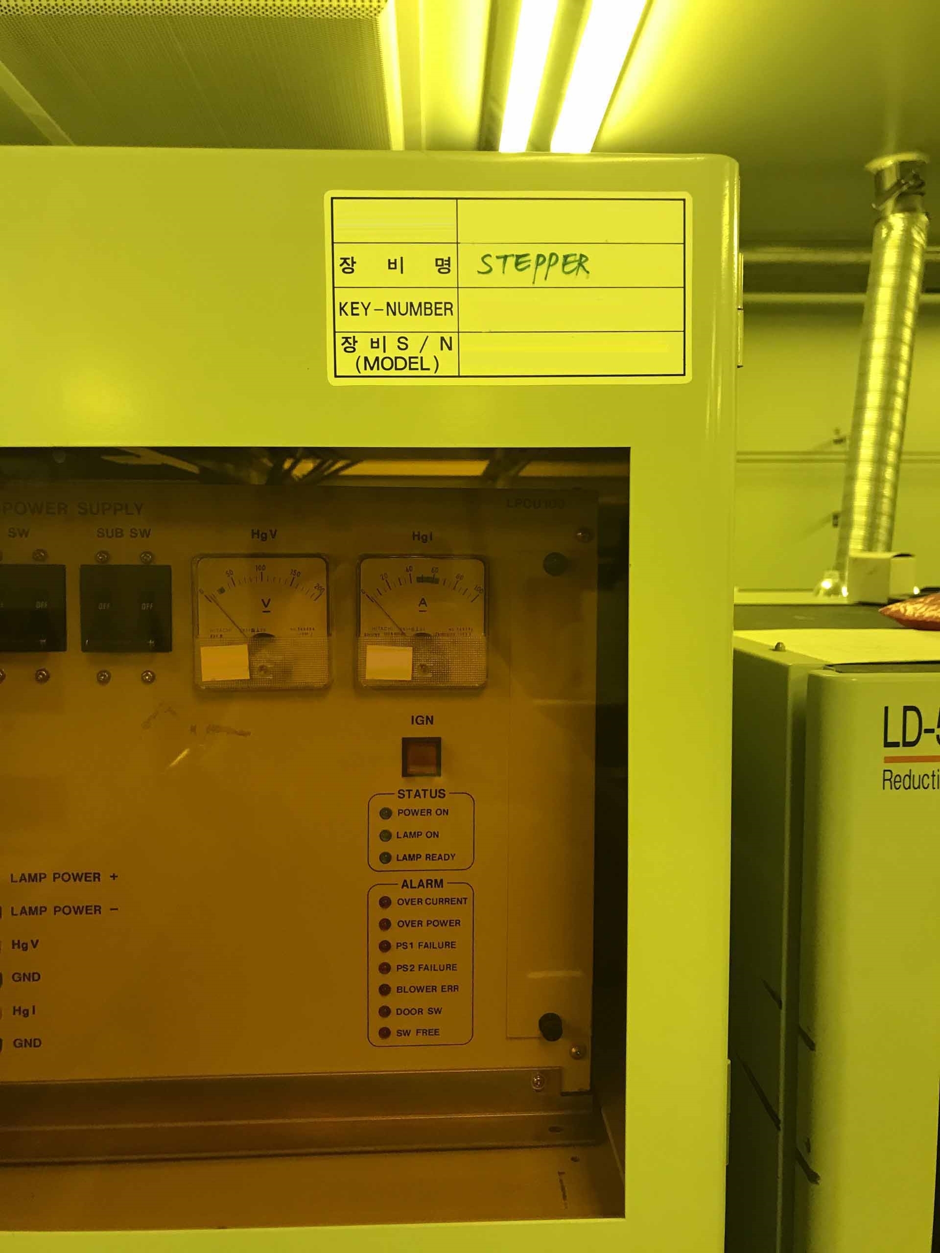


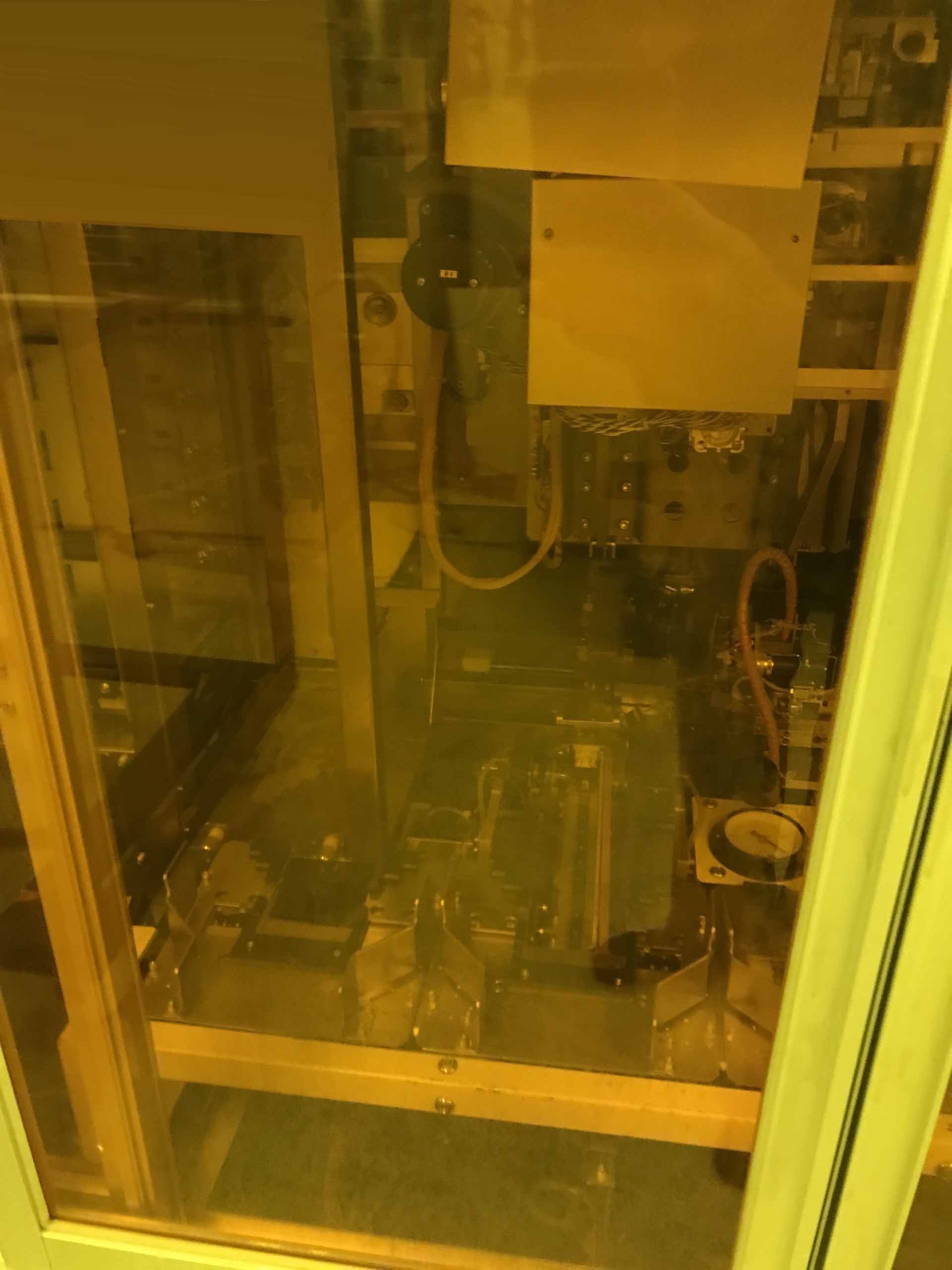

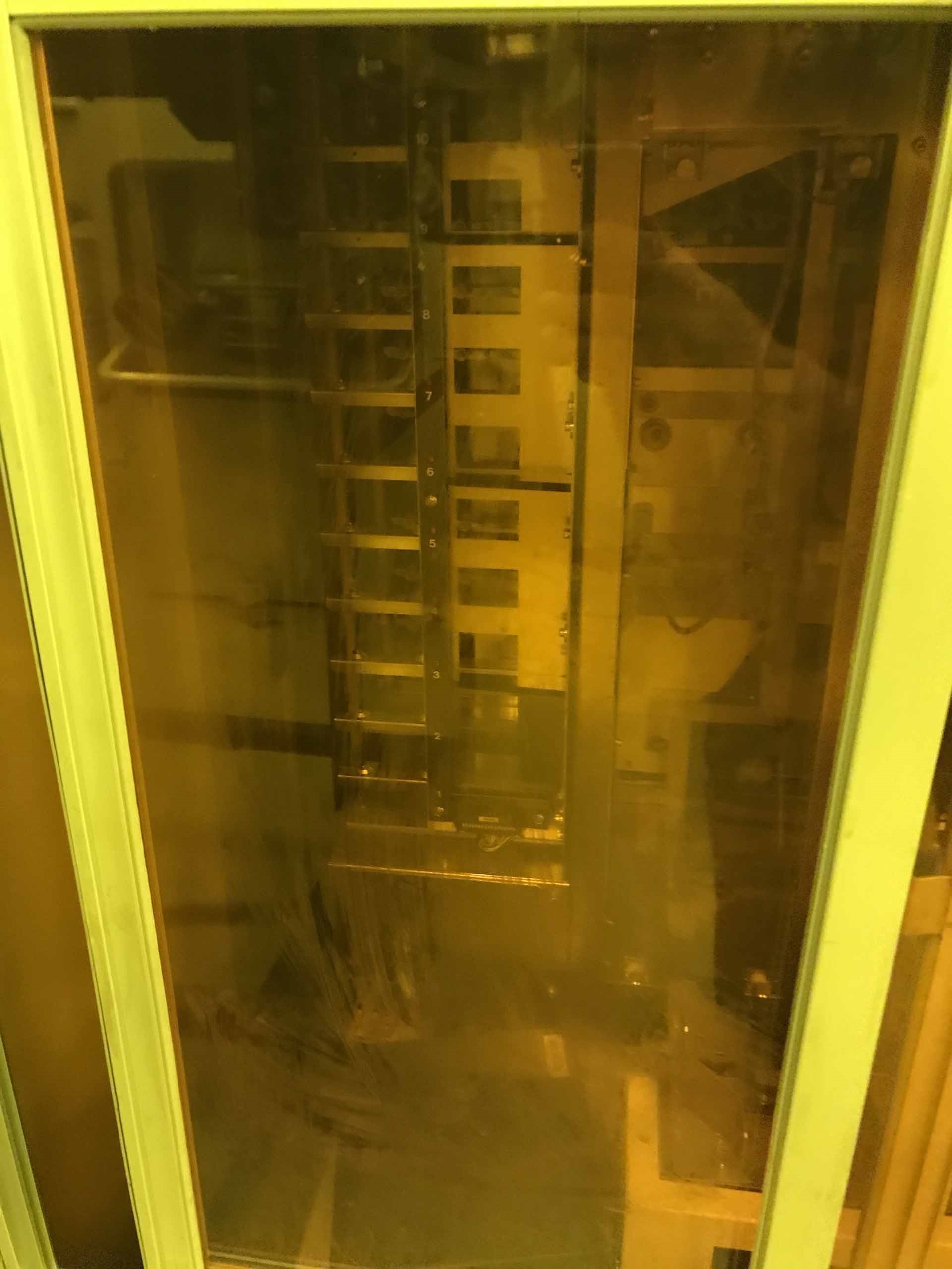

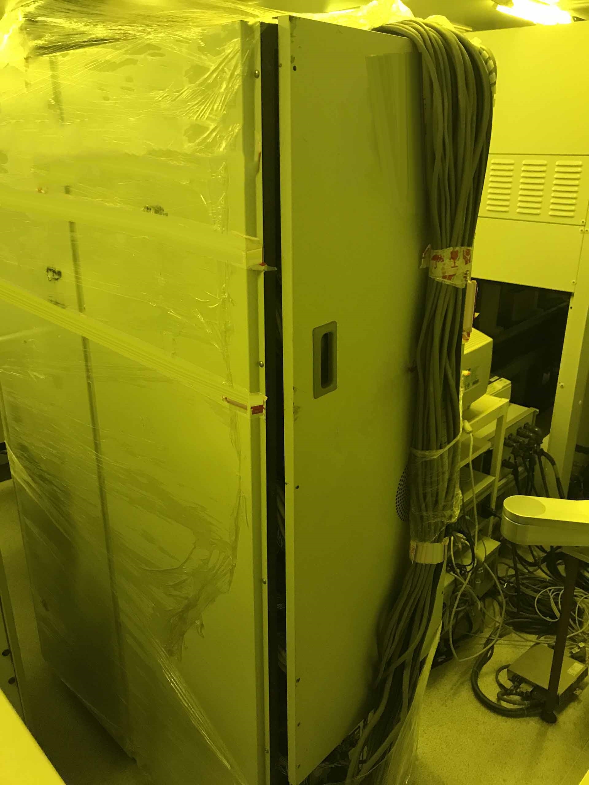

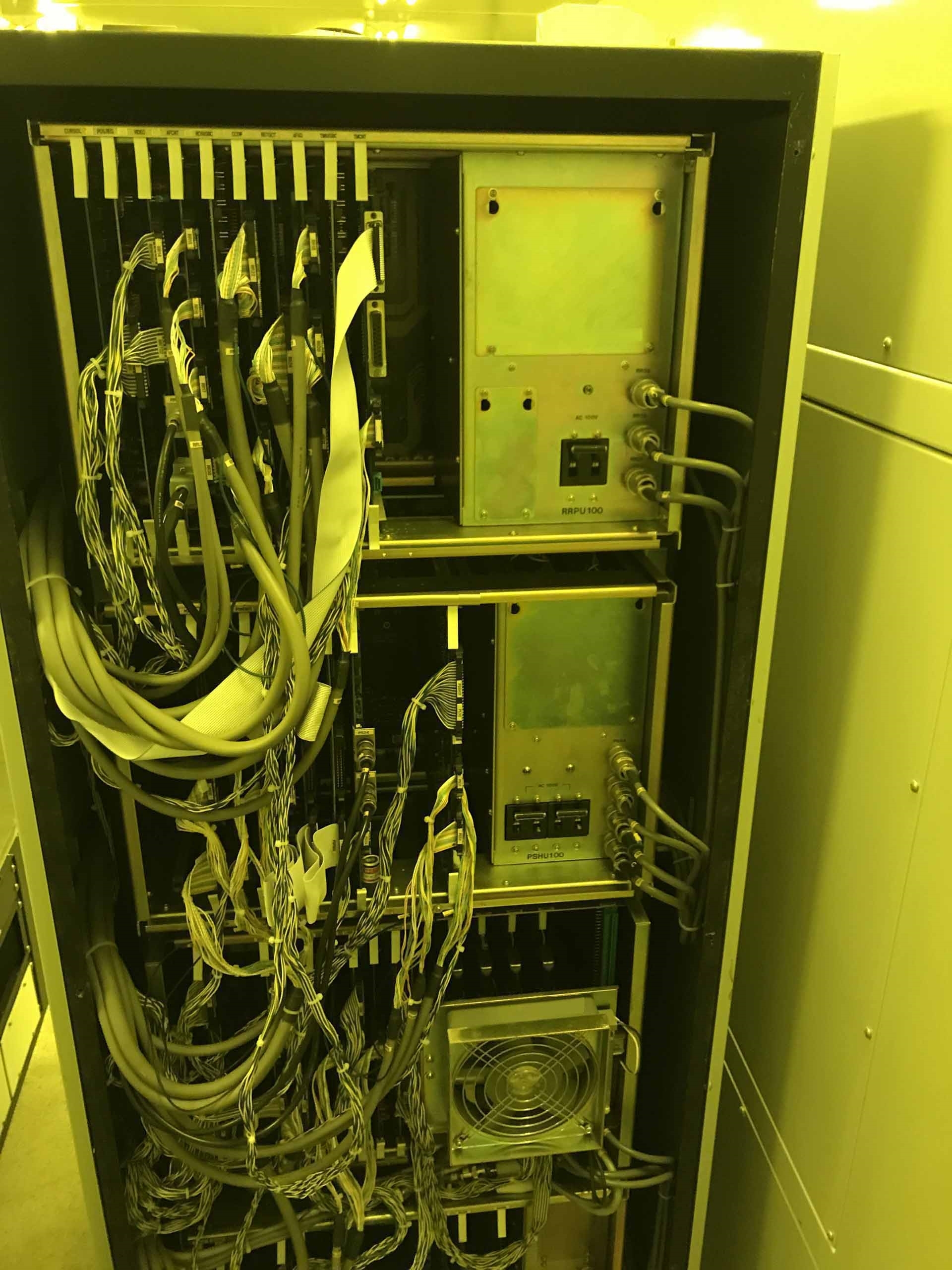

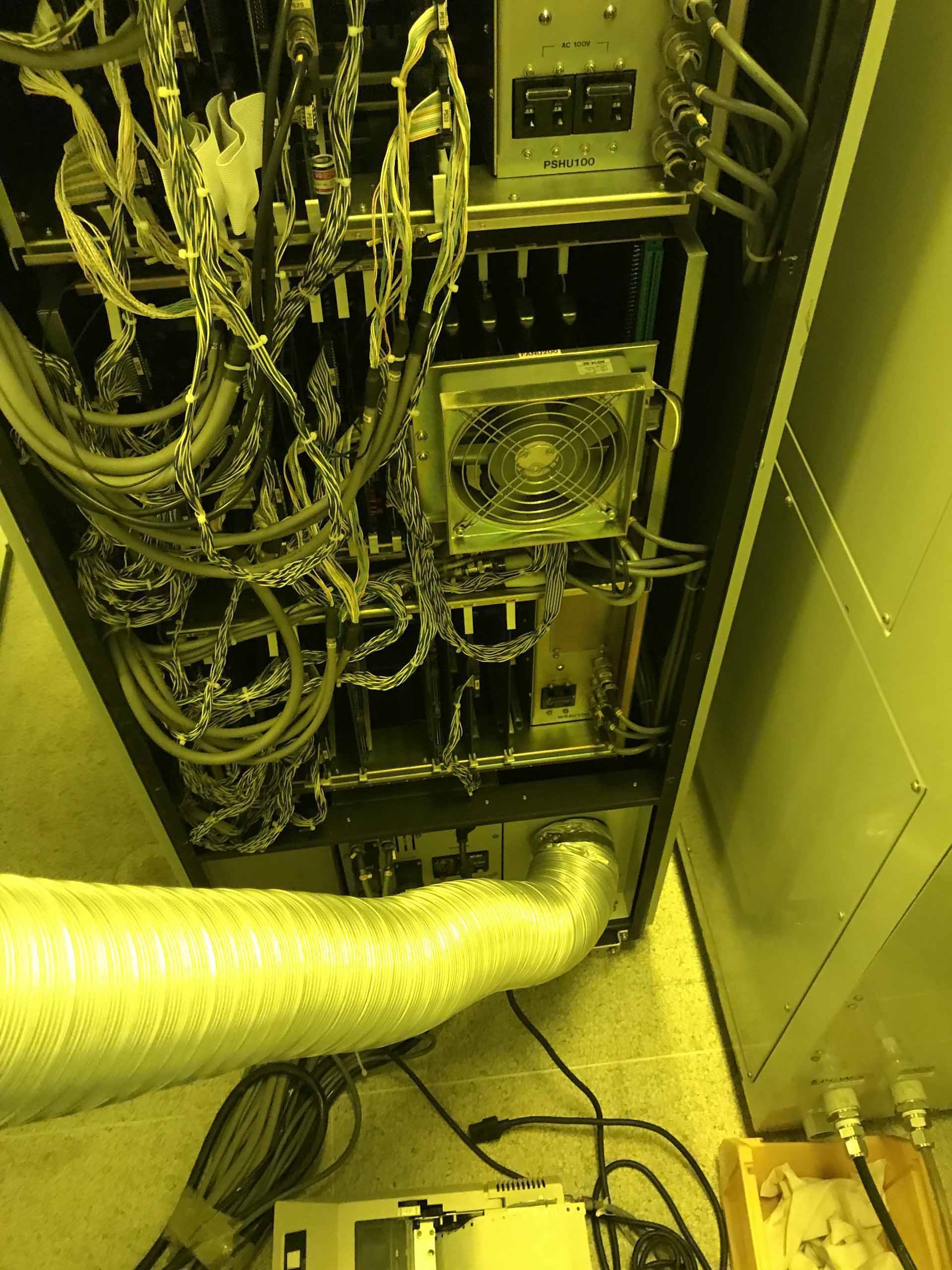


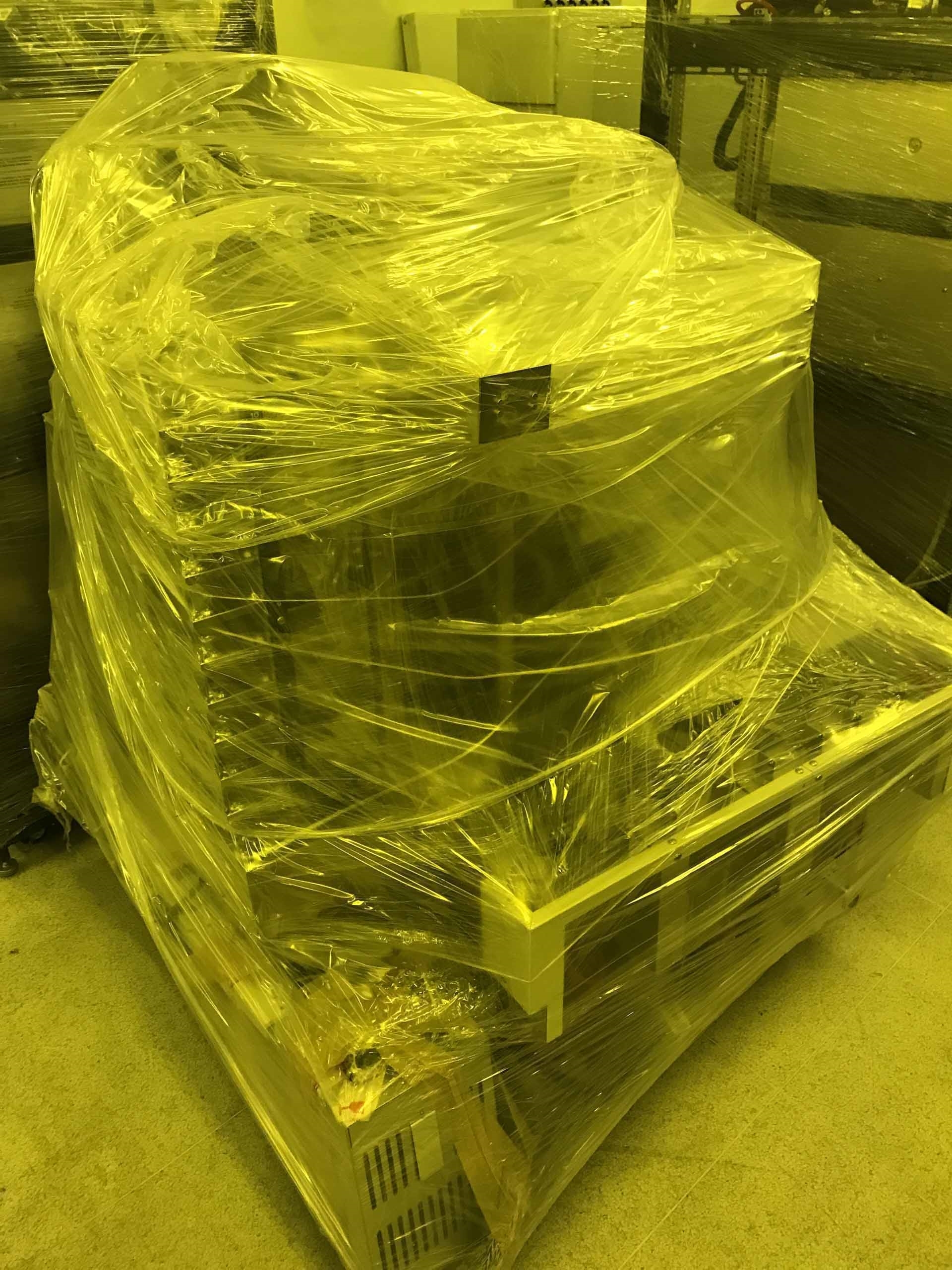


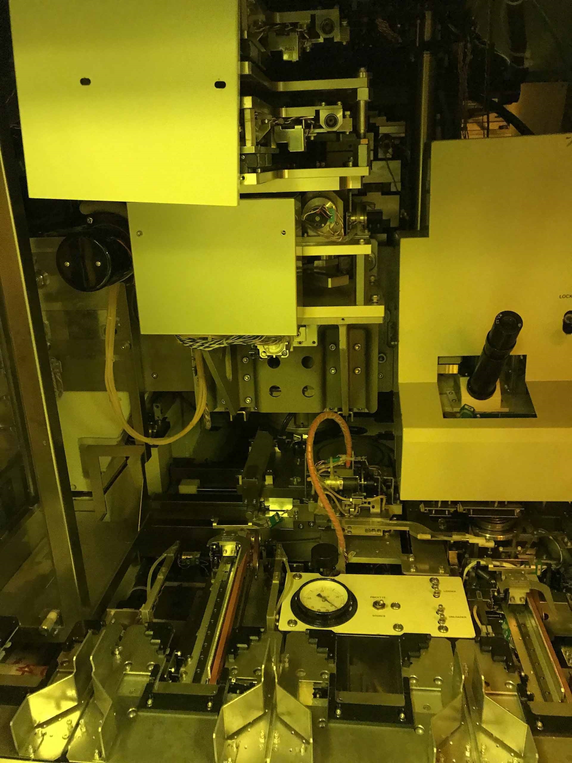

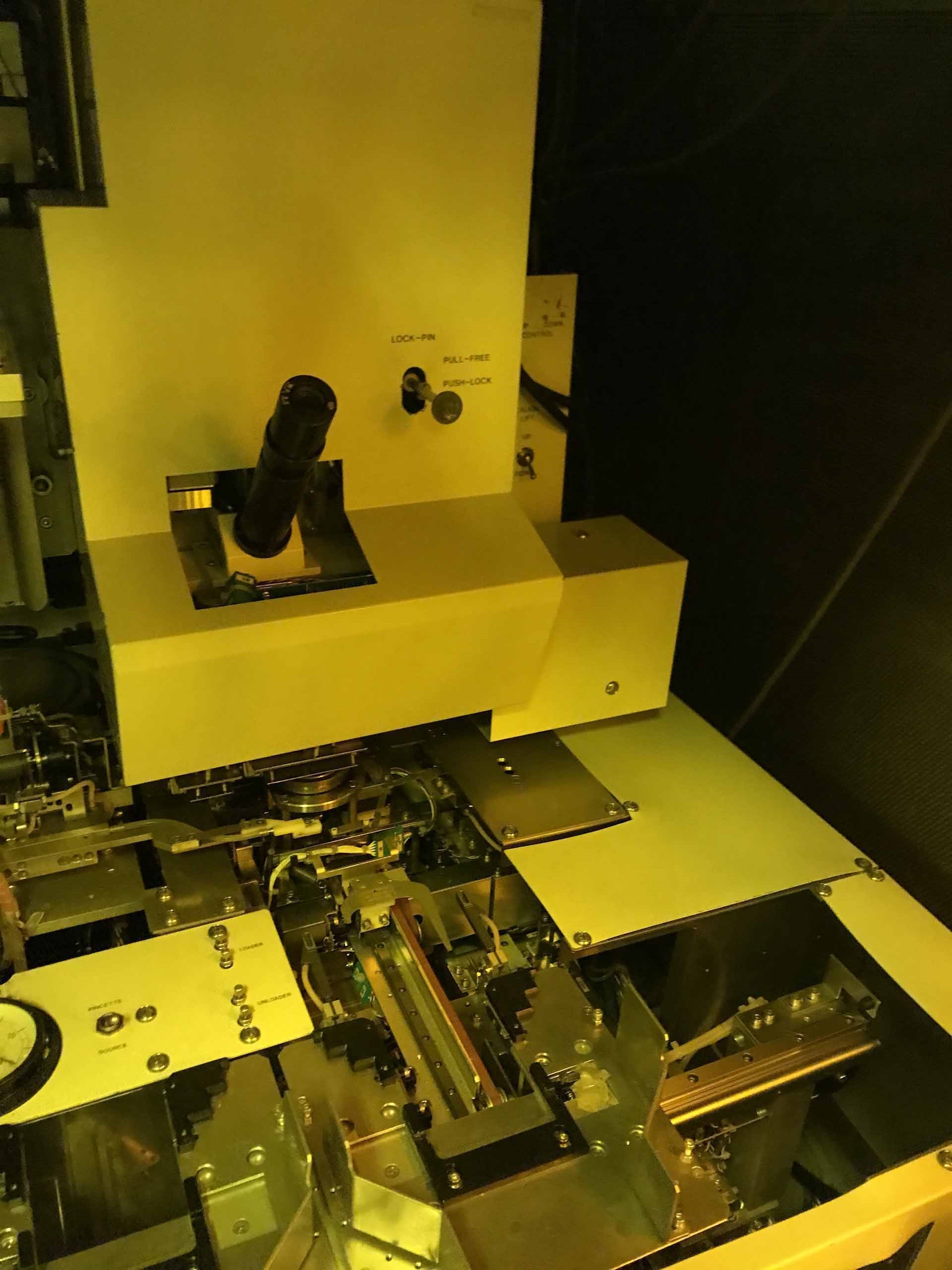

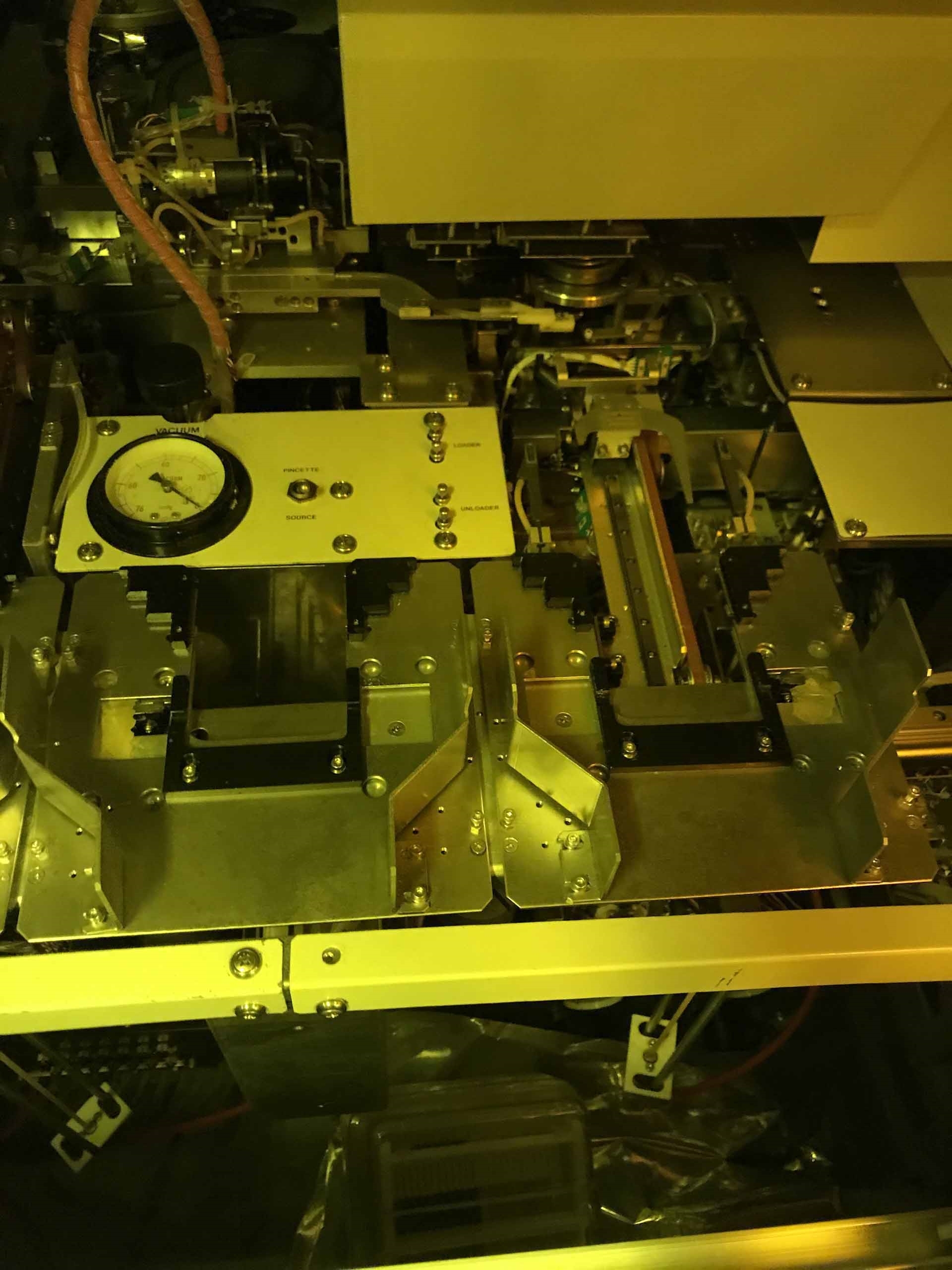


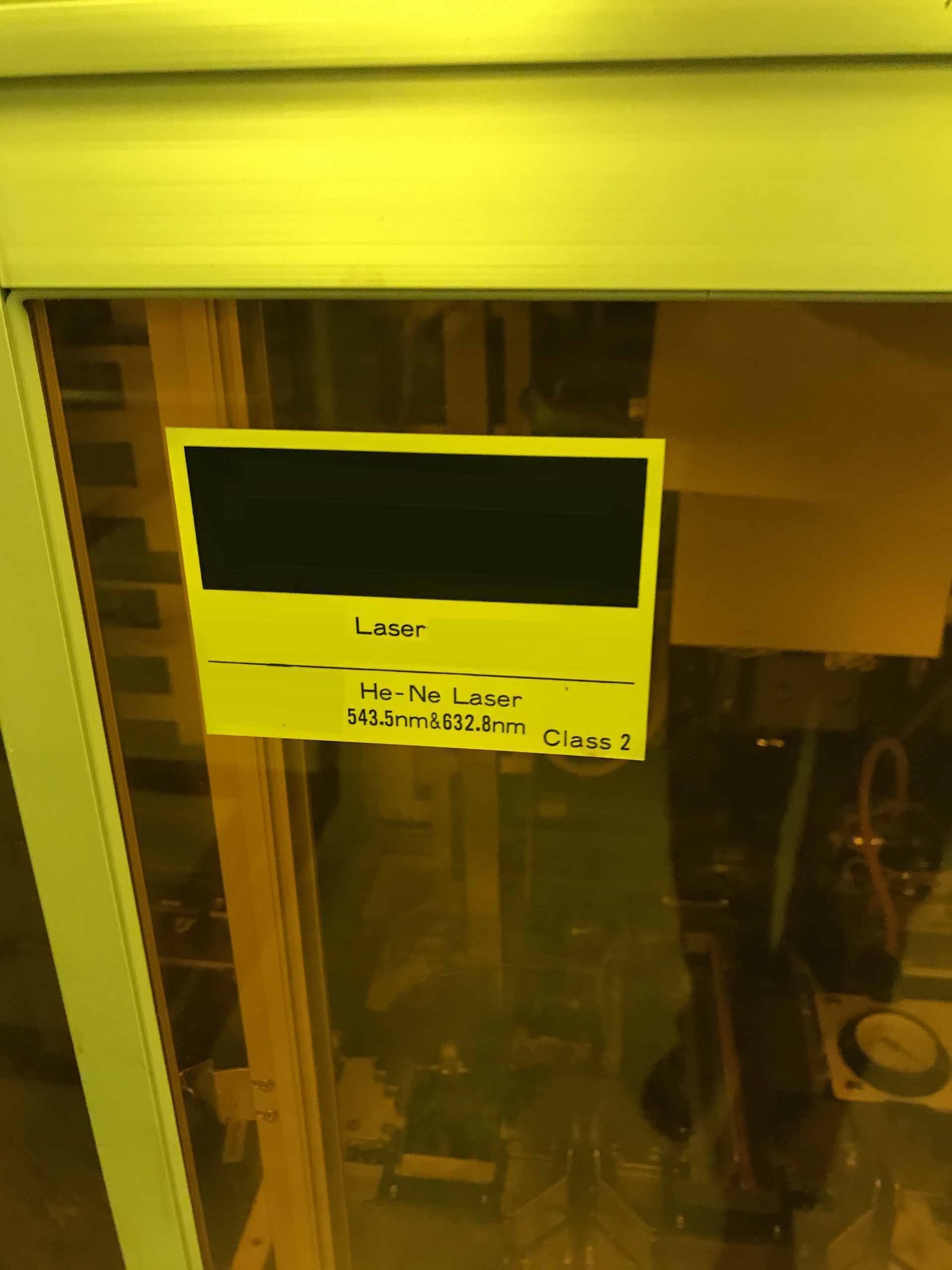

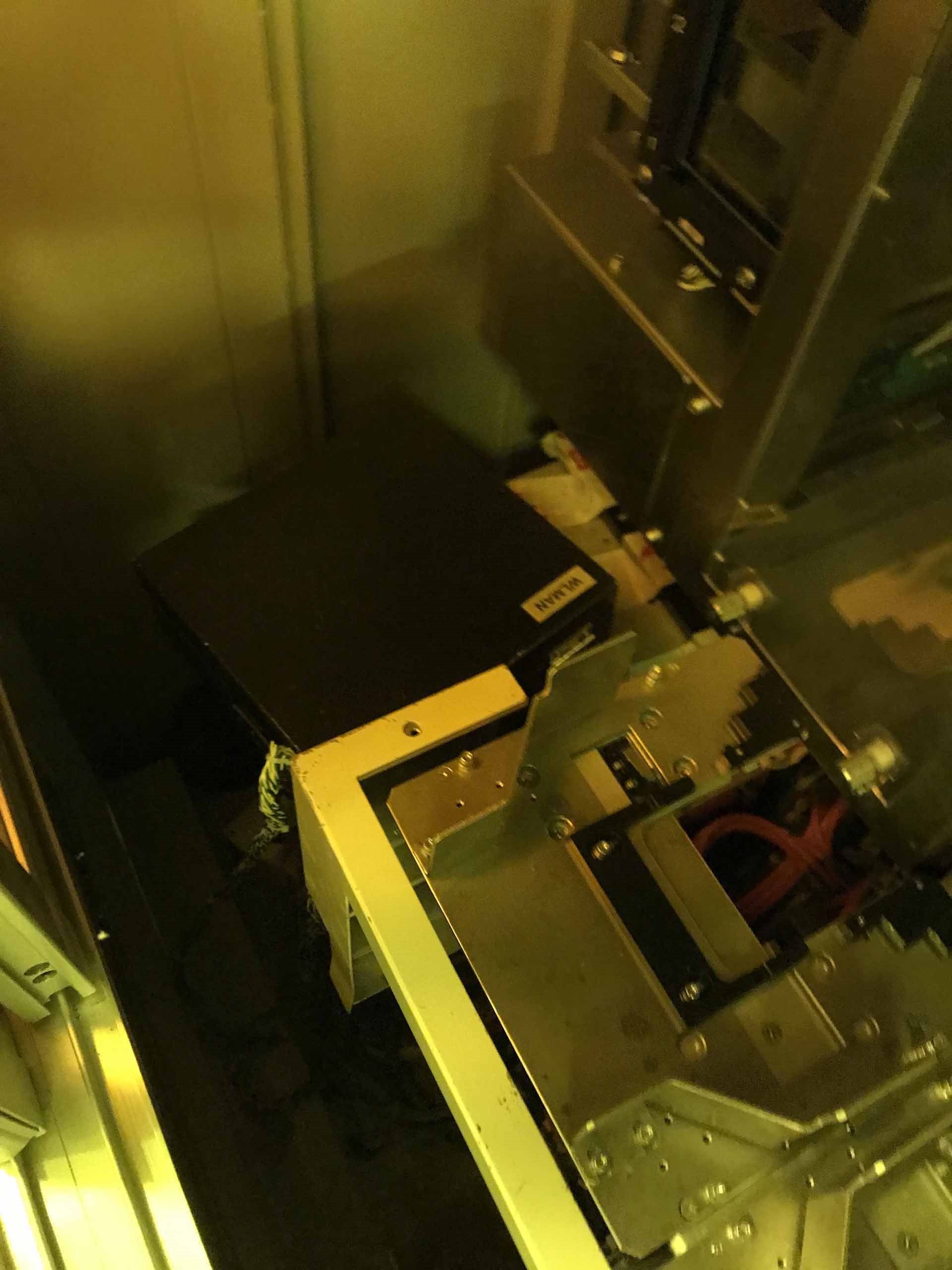

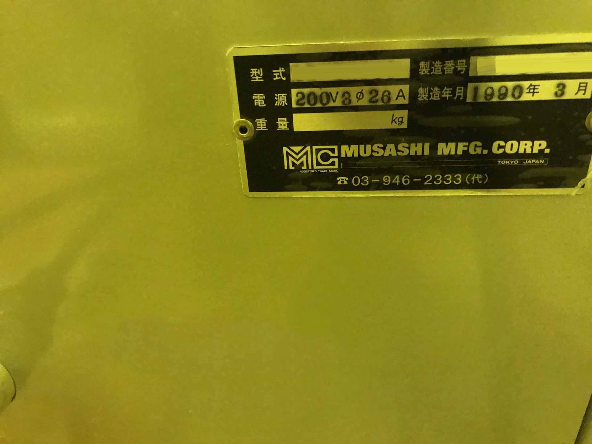

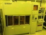
HITACHI LD-5011iA is a wafer stepper designed for state-of-the-art semiconductor device fabrication. This wafer stepper is capable of producing 5-inch (at 200mm) microlithographic images by printing light through a series of aligned reticles. It delivers superior performance and efficiency with its automated, simultaneous lens changing, pattern projection, and alignment functions. LD-5011iA is a step and repeat equipment comprising of an acousto-optic modulator to help with precise reticle positioning as well as focus alignment. With its automated automation pattern projection and wafer alignment systems, it can project and align a large number of patterns on a single wafer. This wafer stepper is equipped with a state-of-the-art, high-resolution optical projection lens that can produce diffraction-limited images of as small as 0.6-micron features. Furthermore, HITACHI LD-5011iA has a high speed along with a high accuracy capability, providing maximal exposure times with excellent image quality. It is also capable of supporting a wide range of exposures and resists allowing the user to optimize processes according to their needs. The system also has a variety of exposure functions that can be used depending on the user's requirements. This includes corner of field security (FSE) for optimal pattern placement accuracies, defect inspection, and fast wafer inspection. Additionally, the model is capable of providing dynamic focus control (DFC) and shot process capability. In addition, LD-5011iA is fitted with an advanced cooling unit, which helps maintain temperature and humidity stability. This machine is an advanced thermal control tool that offers improved homogeneity and uniformity in all environmental conditions. Its He-Cd laser beam source has been specifically designed to provide superior shot success, uniformity, and repeatability resulting in high-quality results. Overall, HITACHI LD-5011iA wafer stepper is a robust, high-performing platform designed for semiconductor microlithography processing. With its numerous features and functions, such as automated lens changing, pattern projection and alignment, and the dynamic focus and shot process control, it is a powerful asset that can provide high throughput, excellent pattern placement accuracy, and superior results.
There are no reviews yet
