Used NIKON Nest 3 #293698905 for sale
URL successfully copied!
Tap to zoom
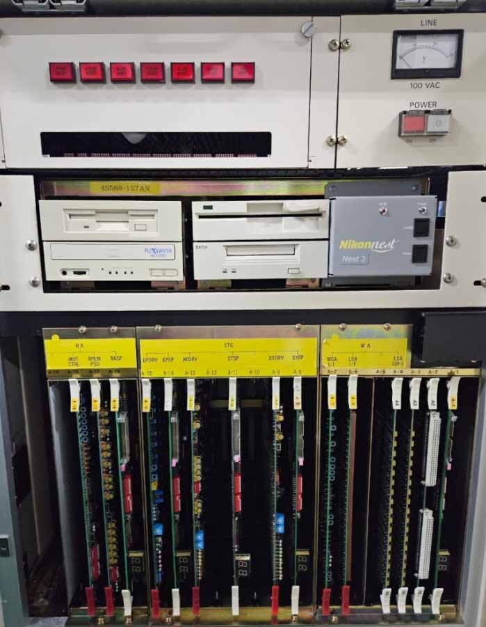

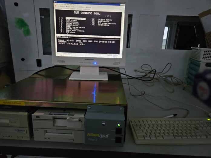
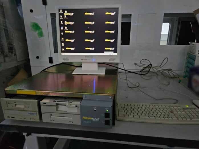
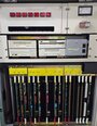
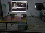
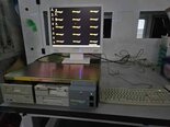
NIKON Nest 3 is a cutting-edge wafer stepper equipment designed for advanced semiconductor manufacturing processes. This state-of-the-art equipment incorporates highly innovative technologies and features to meet the demanding requirements of the semiconductor industry. With its precision, reliability, and flexibility, NIKON NEST3 has become a vital tool in semiconductor fabrication facilities around the world. Nest 3 wafer stepper is equipped with a sophisticated optical system that enables high-resolution patterning on semiconductor wafers. This unit utilizes advanced lithography techniques to transfer intricate patterns from photomasks onto the wafers with exceptional accuracy and consistency. The stepper's optical machine includes a series of high-quality lenses, mirrors, and alignment mechanisms that work together to ensure precise pattern replication across large semiconductor wafers. One of the key features of NEST3 is its advanced alignment and overlay capabilities. The tool incorporates state-of-the-art alignment sensors and algorithms that enable precise registration of the multiple layers of patterns on the semiconductor wafers. This high level of alignment accuracy is crucial for the fabrication of complex integrated circuits with multiple layers of circuitry. NIKON Nest 3 also offers unparalleled flexibility in terms of process control and optimization. The asset is equipped with advanced software that allows semiconductor manufacturers to fine-tune process parameters such as exposure dose, focus, and alignment settings to achieve optimal patterning results. This flexibility enables users to adapt the model to a wide range of semiconductor designs and process requirements. In addition to its advanced patterning capabilities, NIKON NEST3 is designed for high productivity and reliability in semiconductor manufacturing environments. The equipment features a robust wafer handling mechanism that ensures smooth and efficient wafer loading and unloading operations. This reliable wafer handling system minimizes downtime and maximizes the unit's throughput, leading to higher productivity and lower manufacturing costs. Furthermore, Nest 3 incorporates advanced automation features that streamline the semiconductor manufacturing process. The machine is compatible with automated material handling systems and wafer mapping software that enable seamless integration with other equipment in the fabrication facility. This automation capability reduces manual intervention and human errors, resulting in improved process efficiency and yield. Moreover, NEST3 is designed with scalability in mind to meet the evolving needs of the semiconductor industry. The tool can be easily upgraded with additional modules and functionalities to accommodate future technology nodes and semiconductor design requirements. This scalability ensures that semiconductor manufacturers can continue to leverage the capabilities of NIKON Nest 3 for years to come. Overall, NIKON NEST3 represents a revolutionary advancement in wafer stepper technology, offering semiconductor manufacturers unparalleled precision, flexibility, and reliability in the fabrication of advanced semiconductor devices. With its state-of-the-art features and capabilities, Nest 3 has established itself as a leading wafer stepper asset in the semiconductor industry and is poised to drive innovation and productivity in semiconductor manufacturing for years to come.
There are no reviews yet