Used NIKON Nest 3 #293754612 for sale
URL successfully copied!
Tap to zoom
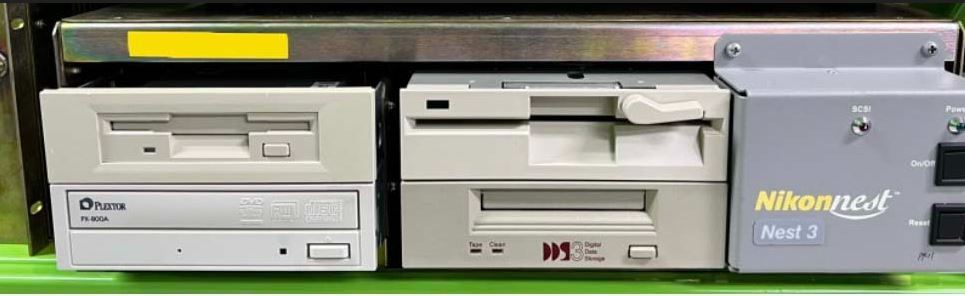

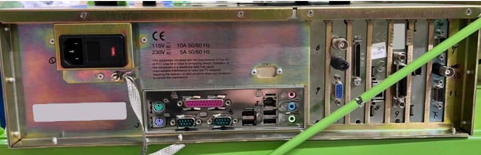
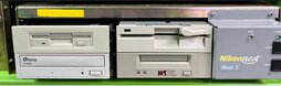
NIKON Nest 3 is a cutting-edge wafer stepper that represents a significant advancement in lithography technology. This tool is designed to fulfill the rapidly evolving demands of the semiconductor industry by offering unparalleled precision, speed, and flexibility in the patterning process. The integration of innovative features and advanced capabilities in NIKON NEST3 ensures superior performance in the production of high-quality semiconductor devices. At the heart of Nest 3 wafer stepper is its state-of-the-art projection optics equipment. This system is responsible for the critical task of projecting the photomask patterns onto the silicon wafer with exceptional accuracy and resolution. The optical design of the projection unit in NEST3 is optimized to achieve submicron resolution, enabling the production of intricate and highly detailed semiconductor devices. The use of cutting-edge materials and coatings in the optics ensures high light transmission efficiency and minimal aberrations, resulting in superior image quality and pattern fidelity. NIKON Nest 3 offers a wide range of exposure modes and control options to accommodate various lithography processes and substrate materials. This flexibility allows semiconductor manufacturers to optimize the patterning process for different device designs and applications. The tool supports both contact and proximity lithography modes, enabling direct pattern transfer onto the wafer surface with high precision and uniformity. Additionally, NIKON NEST3 features advanced alignment and focus control mechanisms that ensure optimal registration and depth of focus, essential for achieving the desired pattern fidelity and process yield. Another key feature of Nest 3 is its advanced automation and software capabilities, which streamline the lithography process and enhance overall productivity. The tool is equipped with intelligent pattern recognition algorithms and feedback mechanisms that enable real-time monitoring and adjustment of exposure parameters for optimal patterning results. The user-friendly interface and intuitive software interface of NEST3 allow semiconductor manufacturers to easily program and execute complex lithography processes with minimal operator intervention. In terms of throughput and productivity, NIKON Nest 3 delivers industry-leading performance characteristics. The tool is designed for high-volume manufacturing environments, with robust components and subsystems that ensure reliable operation and minimal downtime. NIKON NEST3 features a fast and precise stage machine that enables rapid wafer positioning and exposure, leading to shorter cycle times and higher output. The tool also offers a large field of view and exposure area, allowing for the simultaneous patterning of multiple devices on a single wafer, further increasing throughput and efficiency. Overall, Nest 3 wafer stepper represents a pinnacle of lithography technology, offering semiconductor manufacturers a versatile and high-performance solution for producing advanced semiconductor devices. With its advanced optics, flexible exposure modes, sophisticated automation, and high throughput capabilities, NEST3 sets a new standard for precision and efficiency in semiconductor lithography, empowering manufacturers to meet the demanding requirements of modern semiconductor markets.
There are no reviews yet