Used NIKON NSR 1505 G6 #293778039 for sale
URL successfully copied!
Tap to zoom
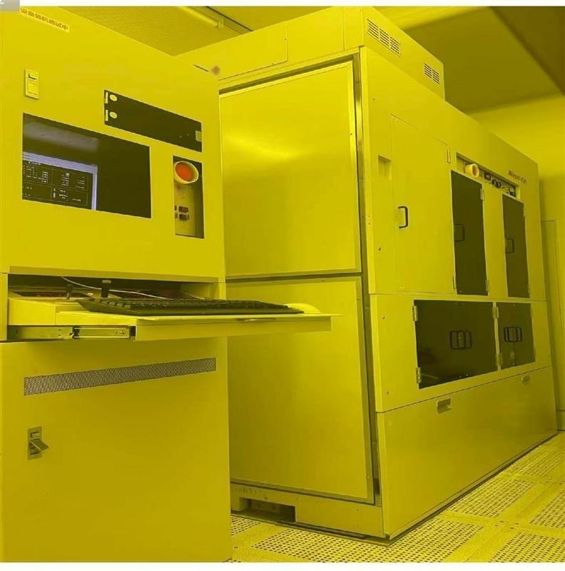

NIKON NSR 1505 G6 is a currently used wafer stepper, designed to produce micro-structures on silicon wafers. The device can facilitate the creation of microchips and other miniaturized electronic components used in a variety of fields. At the core of NSR 1505 G6 wafer stepper is a two-stage reduction lens. The lens has a wide expansive field of view with a maximum scan length allowance of 360 mm and a minimum of 1.5 mm. The beam is managed via a four-mirror equipment and can be used to create patterns on the wafer from a variety of data sources. NIKON NSR 1505 G6's maximum pattern size is 5 μm. The device uses a Reactive Ion Etching (RIE)based pattern transfer system. The scanning stage of NSR 1505 G6 can accurately position and align the wafer for processing. The stage is capable of moving the wafer up to 200mm in both the X and Y-axes with a step size down to 0.2 μm. During the opreation of the device, the positional accuracy of the beam and wafer is ±0.5 μm or better so that the patterns produced are precise and of consistent quality. NIKON NSR 1505 G6 wafer stepper also features an auto-focus unit that allows the user to quickly adjust the focus control settings to assure optimal focus throughout the entire process. The device also boasts a highly efficient particle beam control machine that detects and suppresses particles generated when exposed to gaseous substances, improving the overall fidelity of the patterns being produced. NSR 1505 G6 is constructed from durable materials and capable of withstanding shock and vibration up to 500 m/s2, making it ideal for use in a production environment. The device comes with a user-friendly operator interface that allows for intuitive operation and automation, and can be connected to computers for better control and easier management of multiple steps in the process. Overall NIKON NSR 1505 G6 wafer stepper is a reliable and precise instrument, capable of accurately producing a range of patterns on silicon wafers with precise repeatability. The device is highly modular and can be connected to other elements of production and automated to increase efficiency and throughput, making it a great option for anyone looking to create precise structures on silicon wafers.
There are no reviews yet