Used NIKON NSR 1755 i7A #293681792 for sale
URL successfully copied!


Tap to zoom
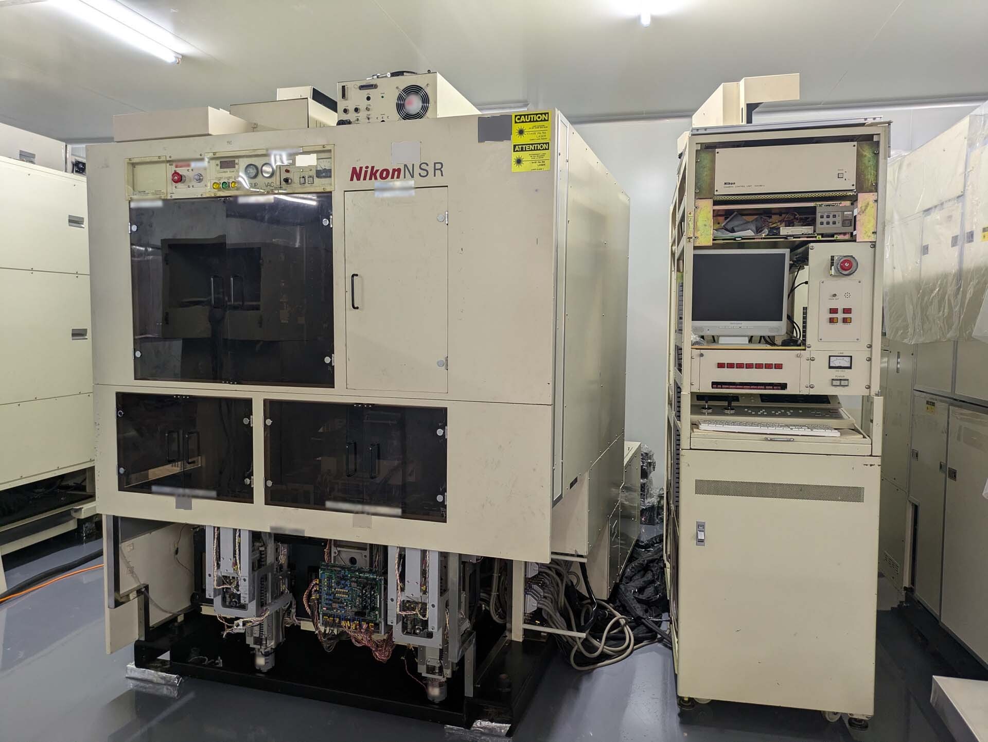

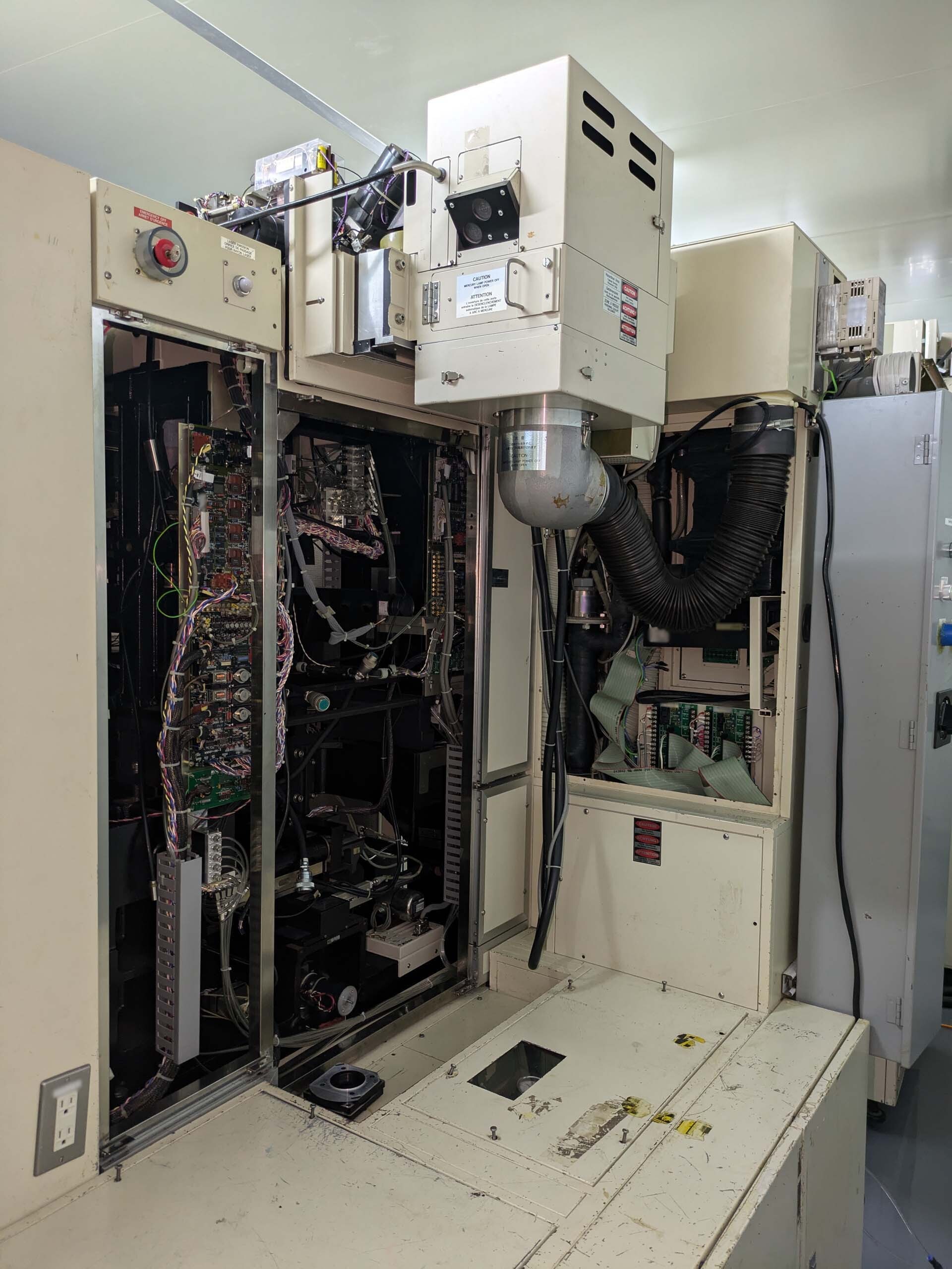
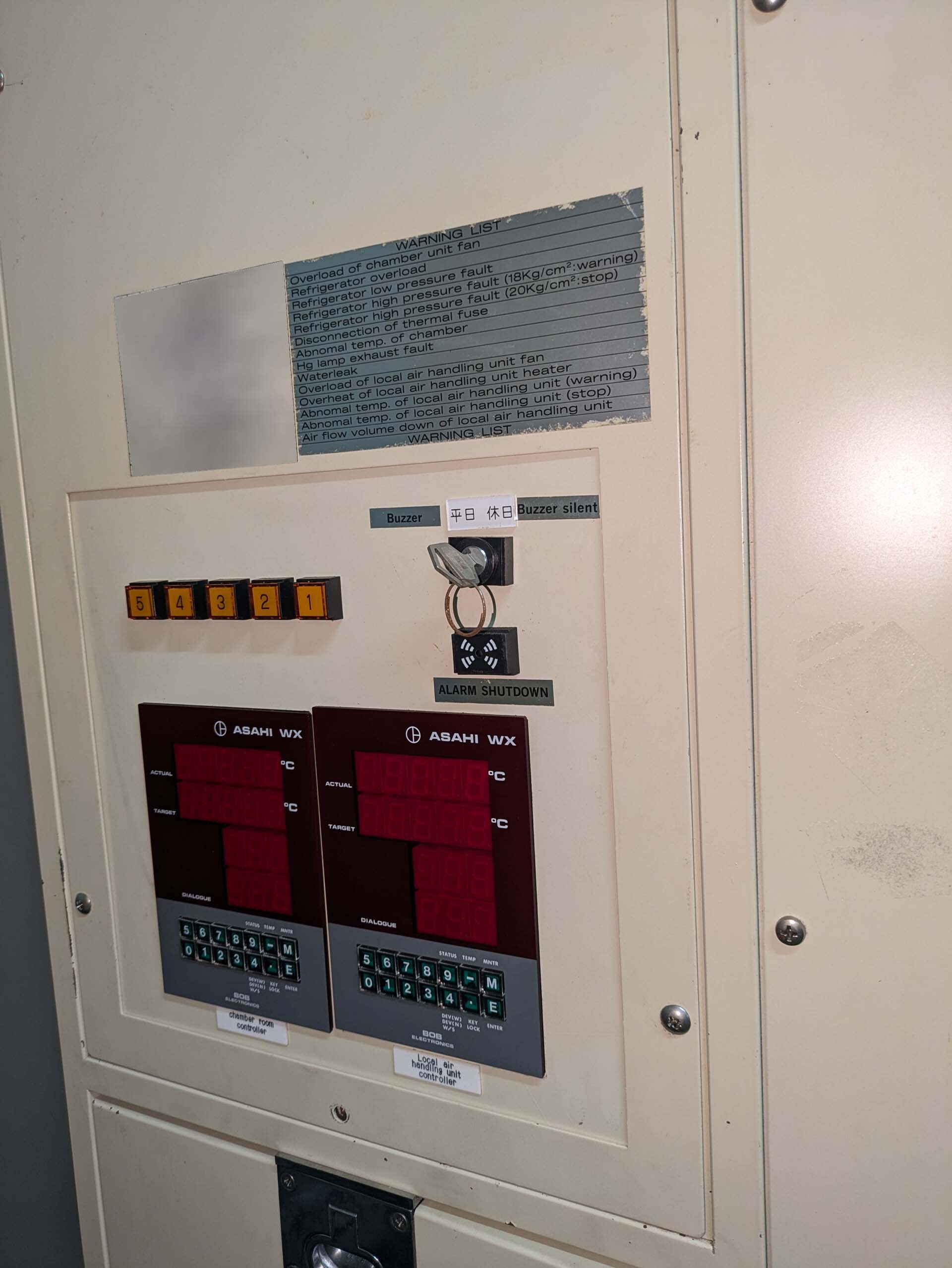
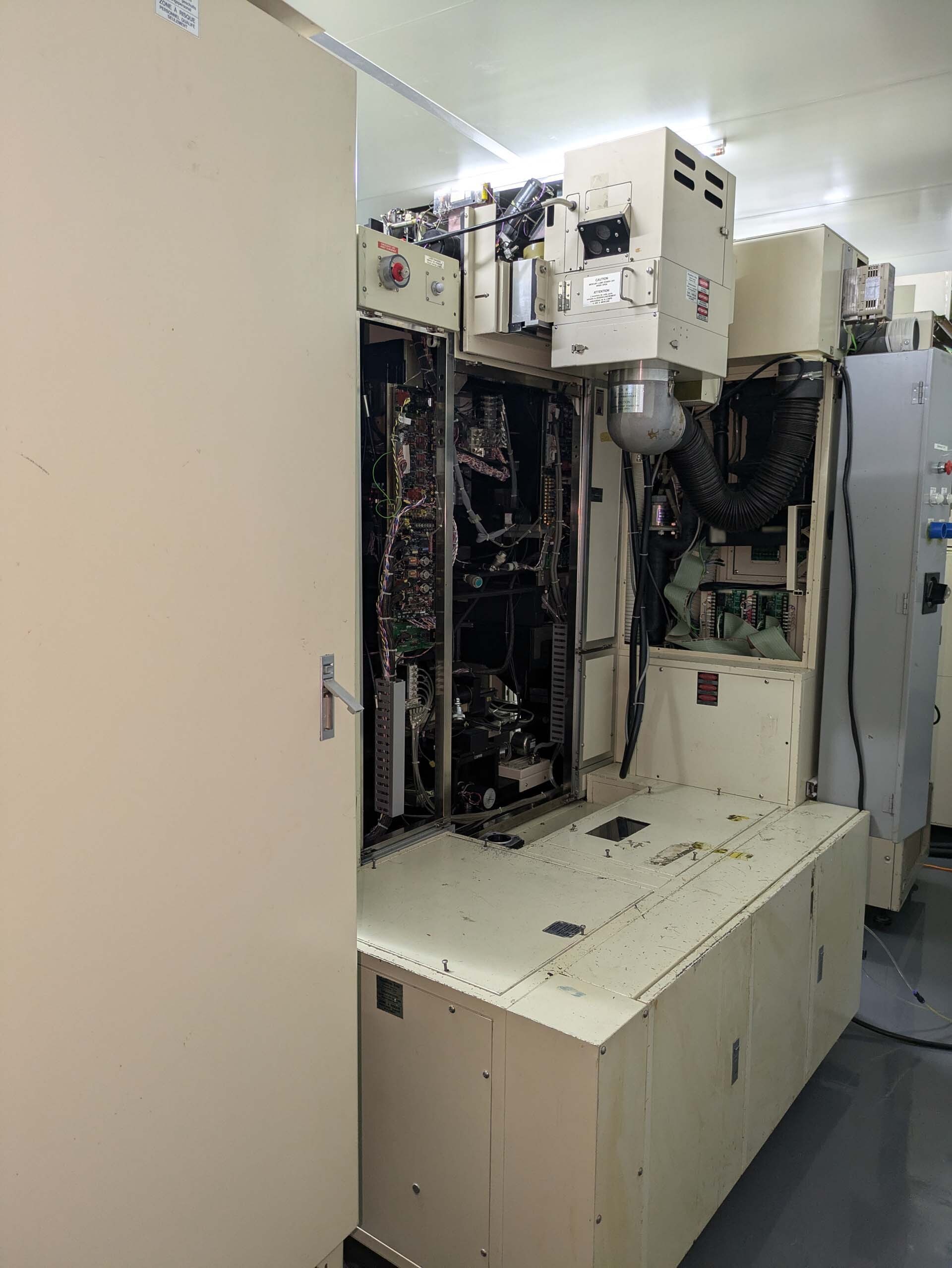
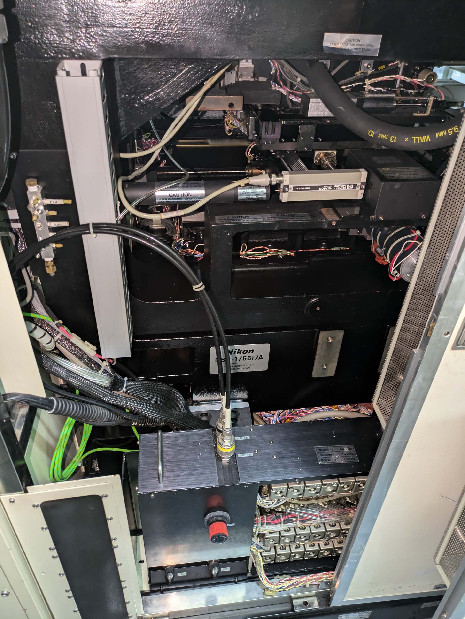
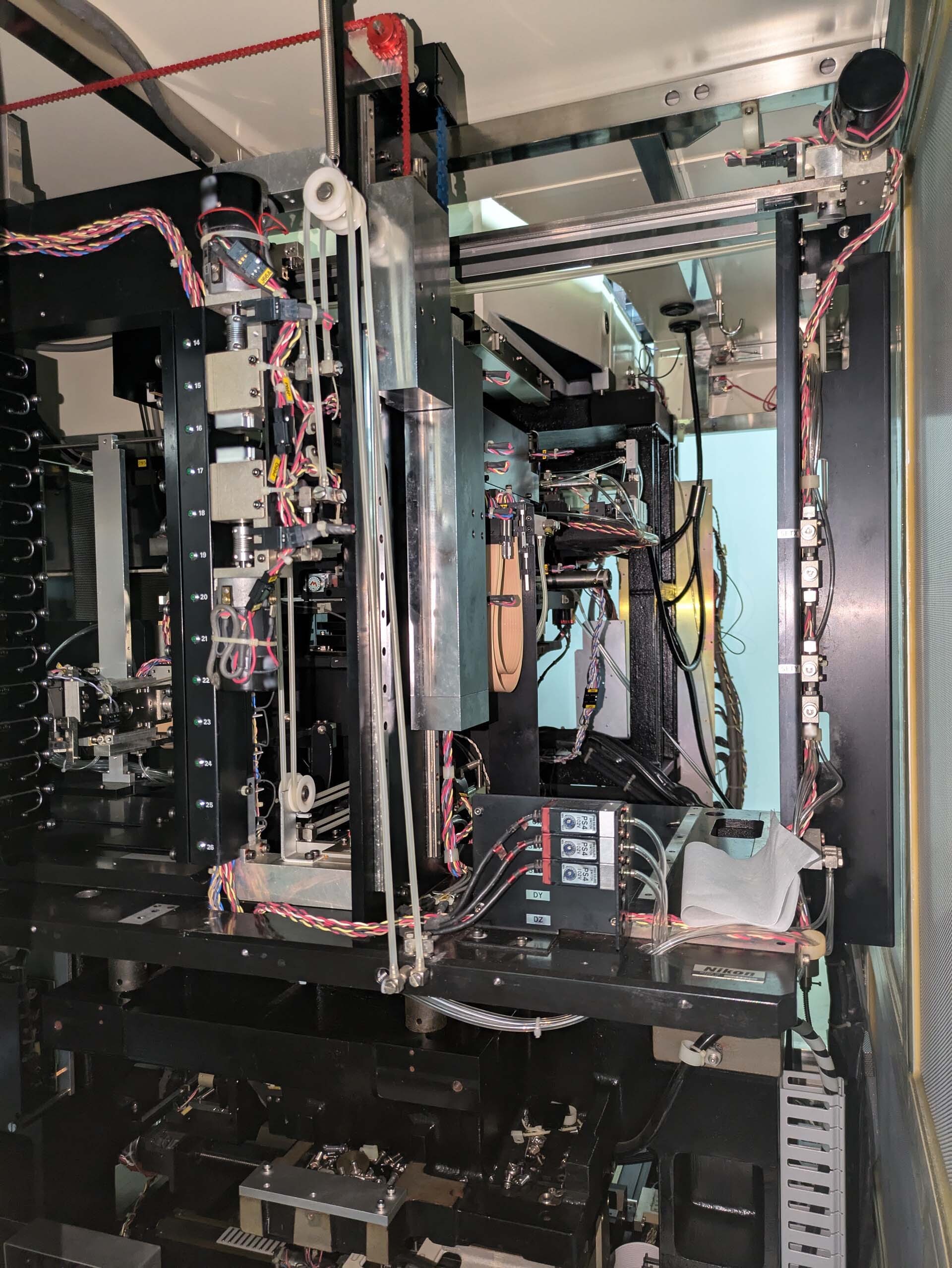
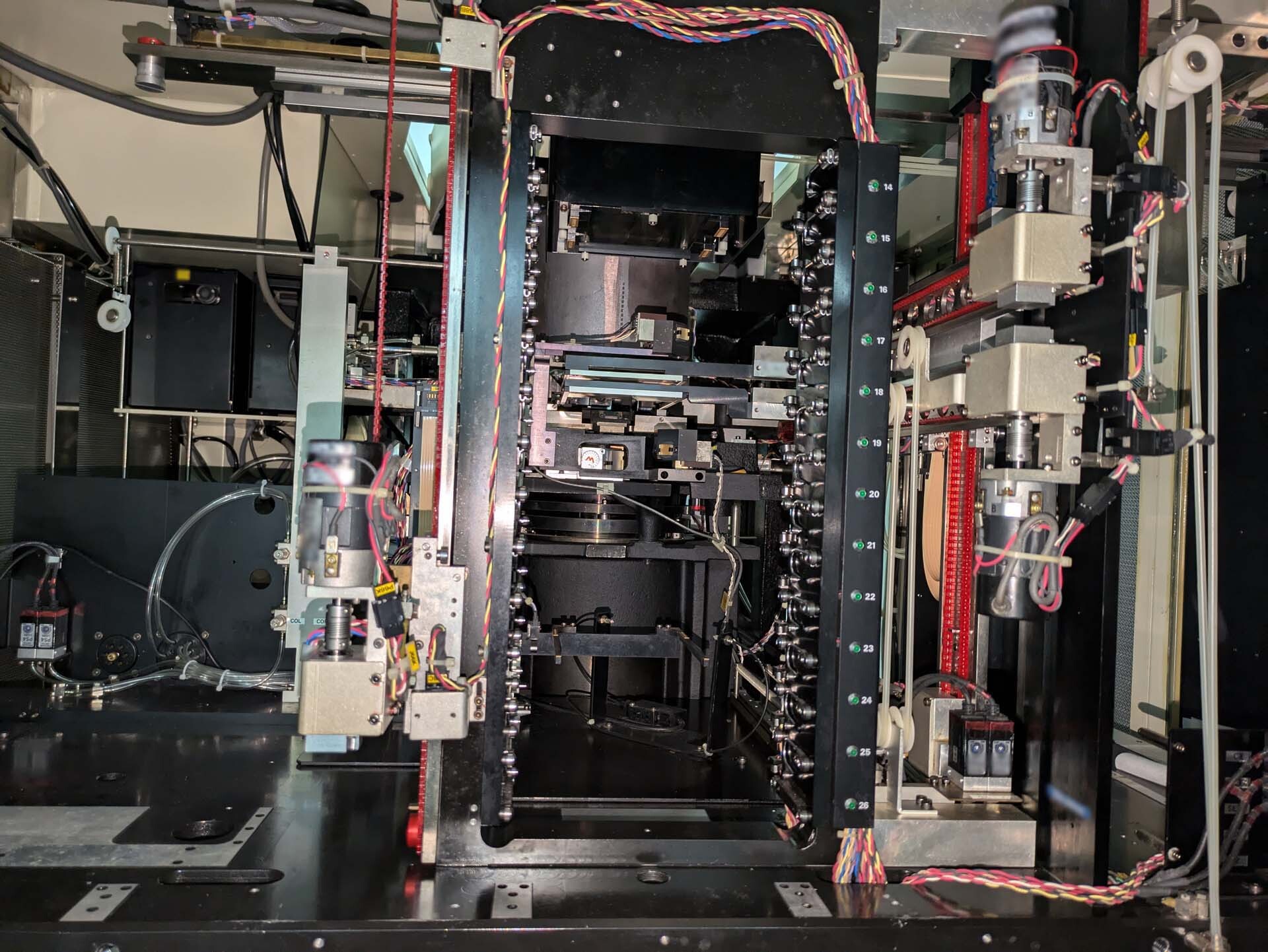
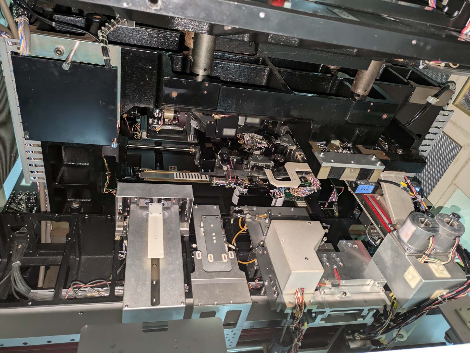
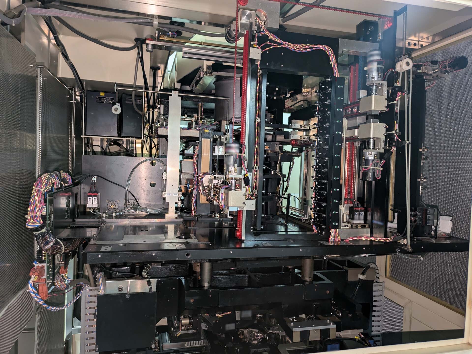
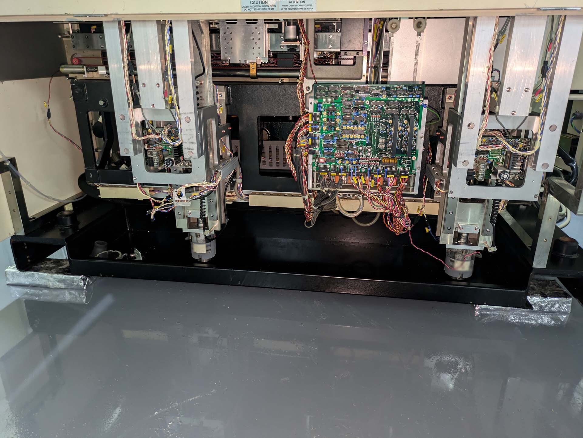
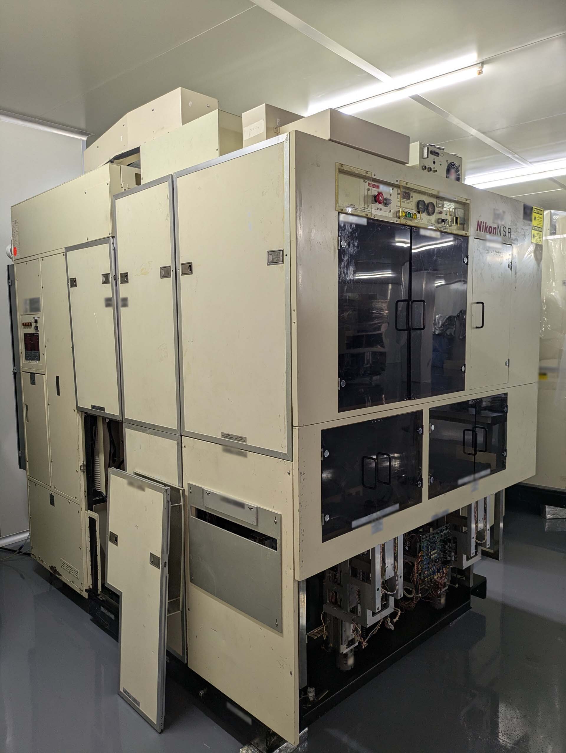
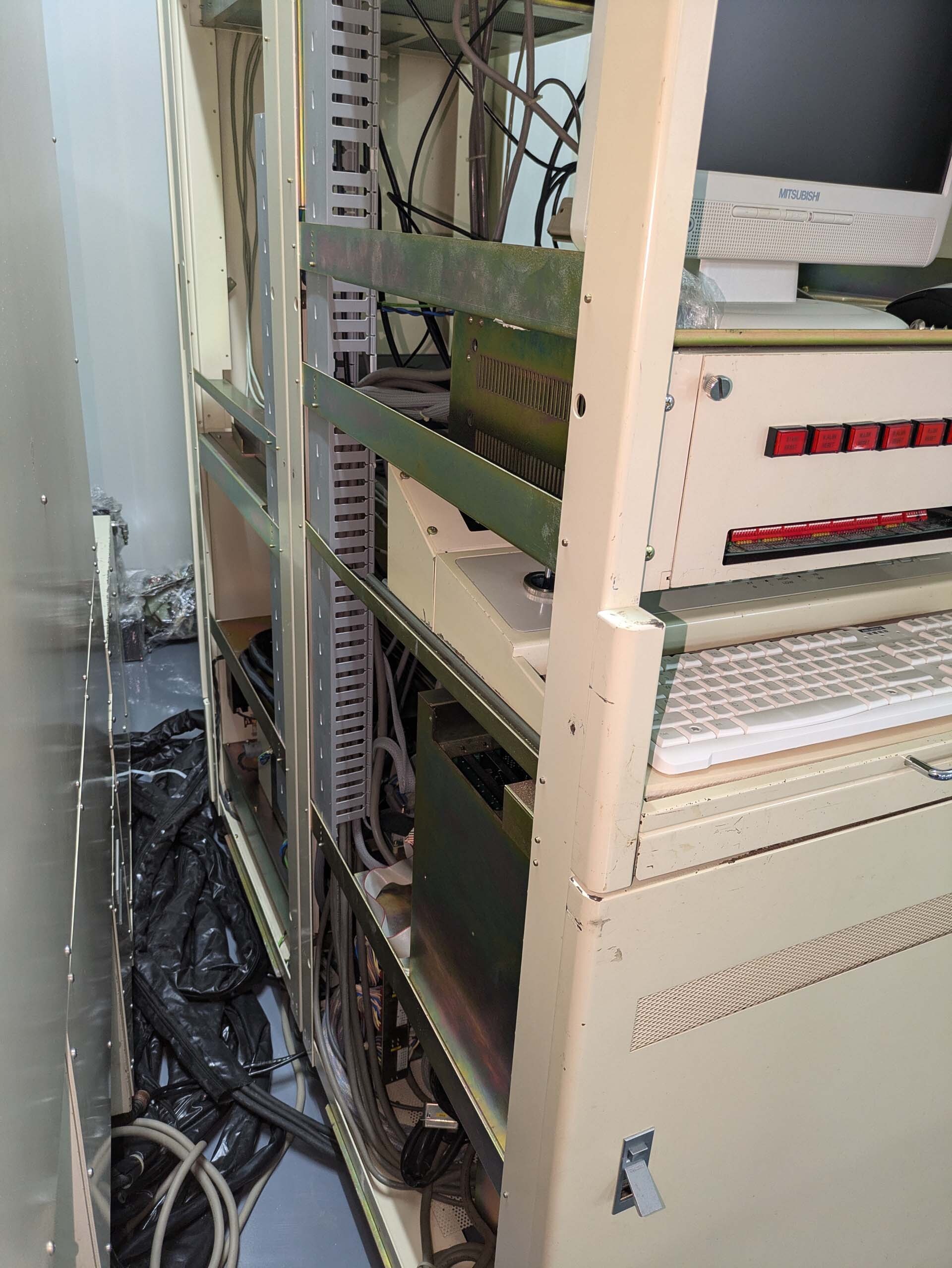
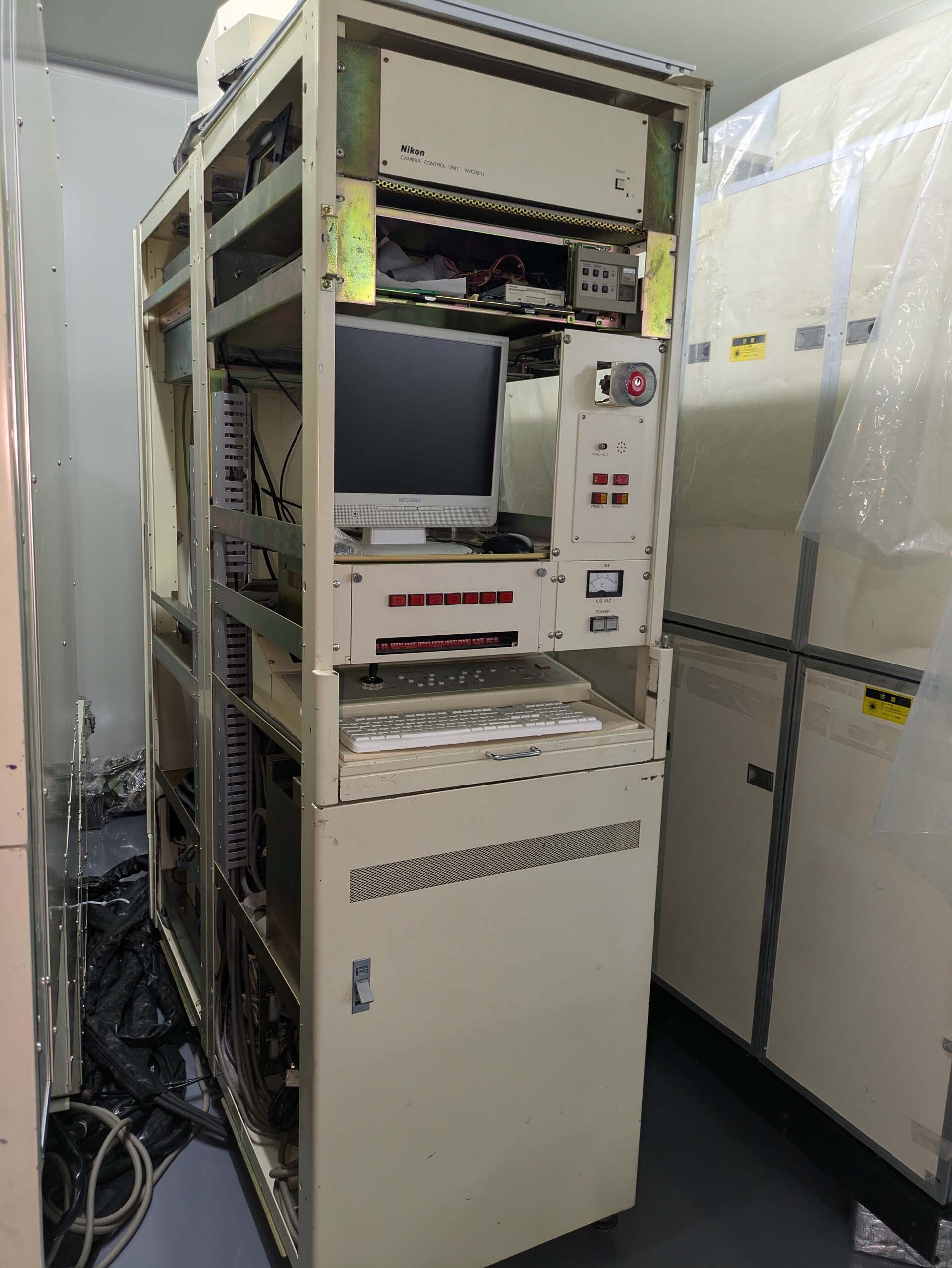
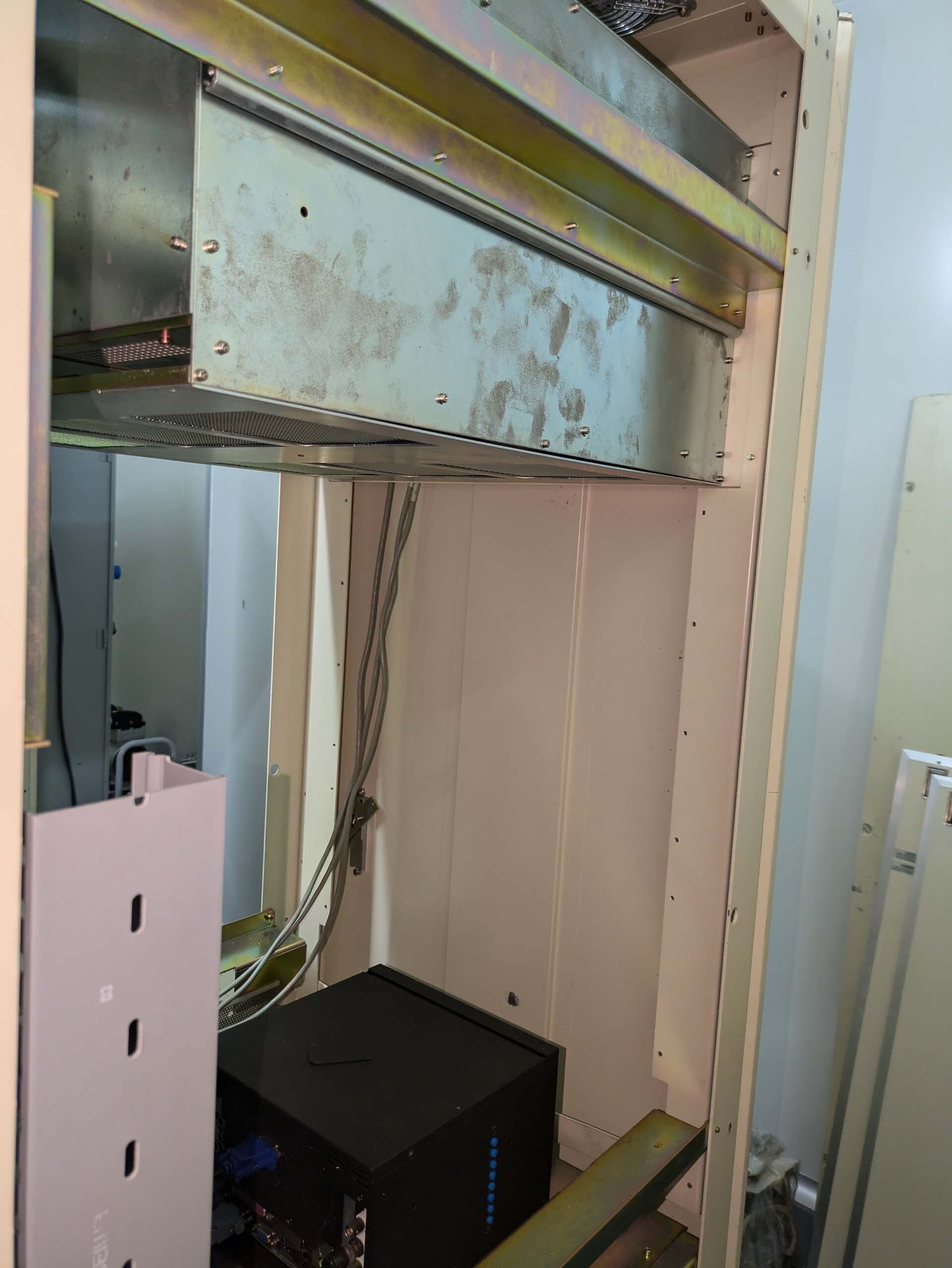
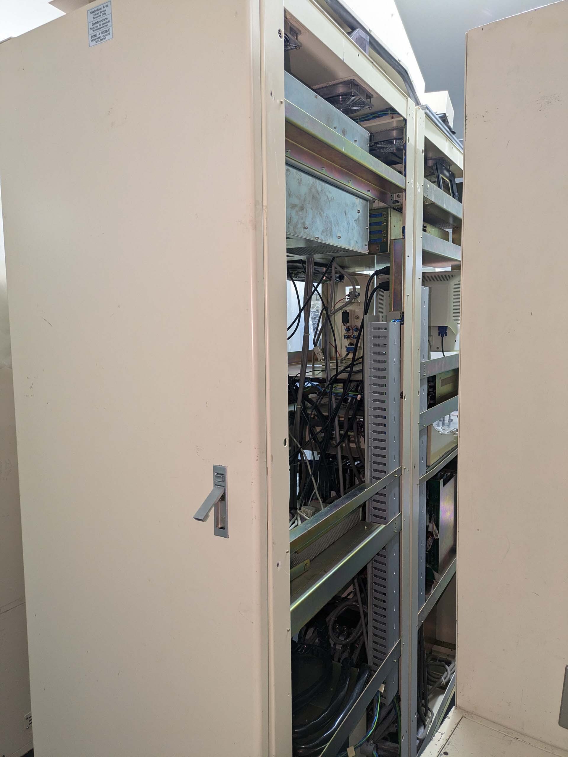
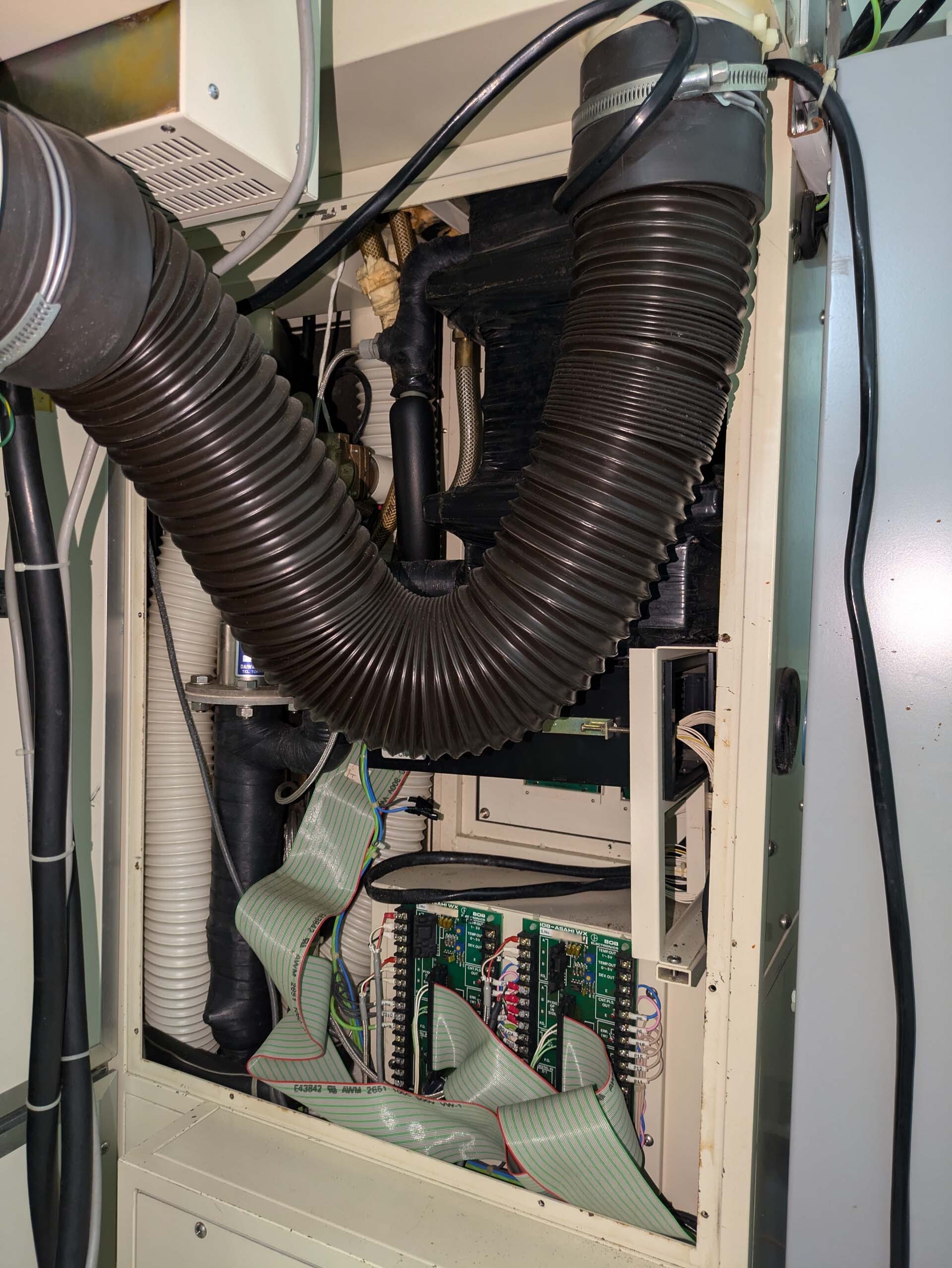
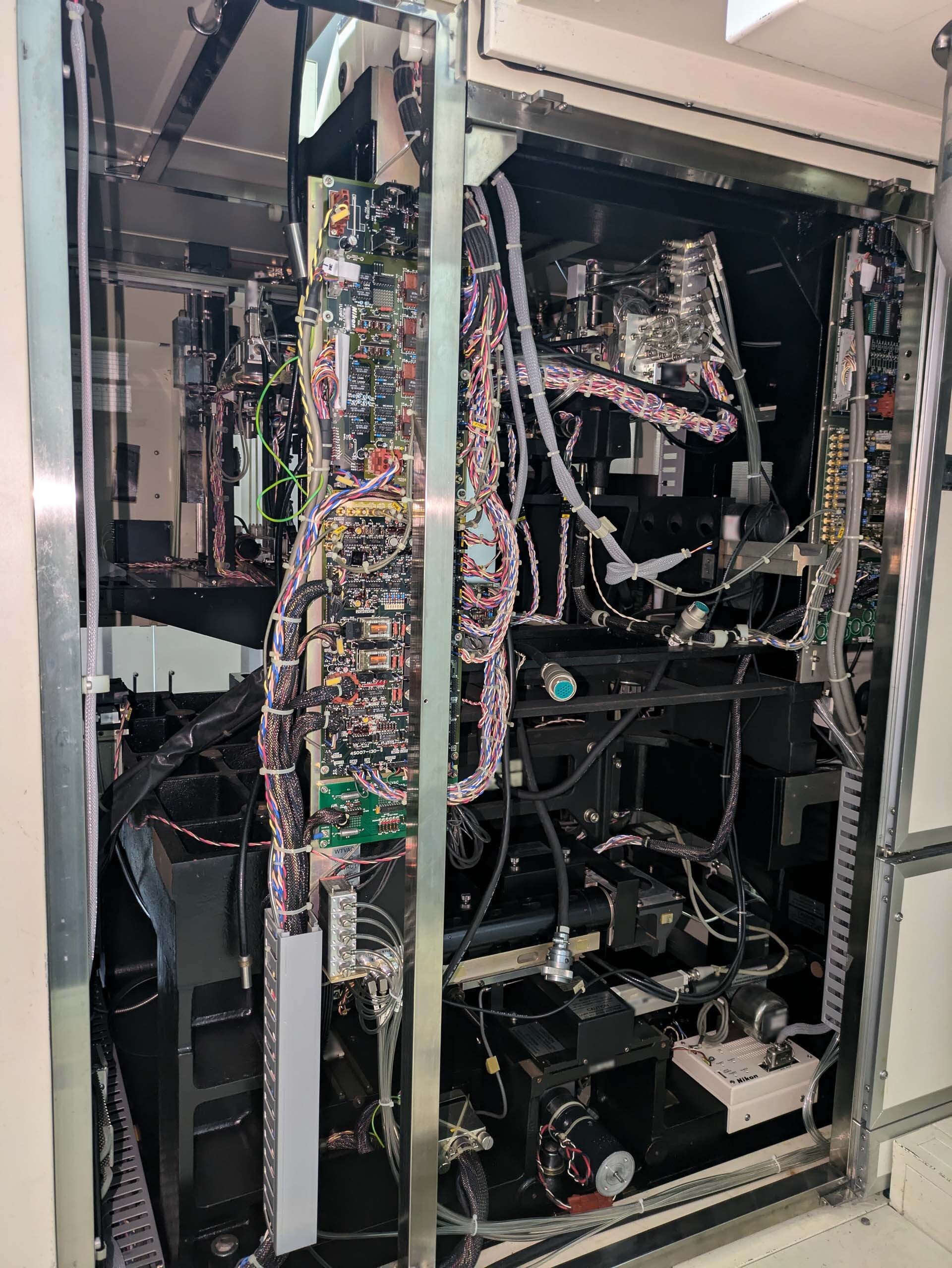
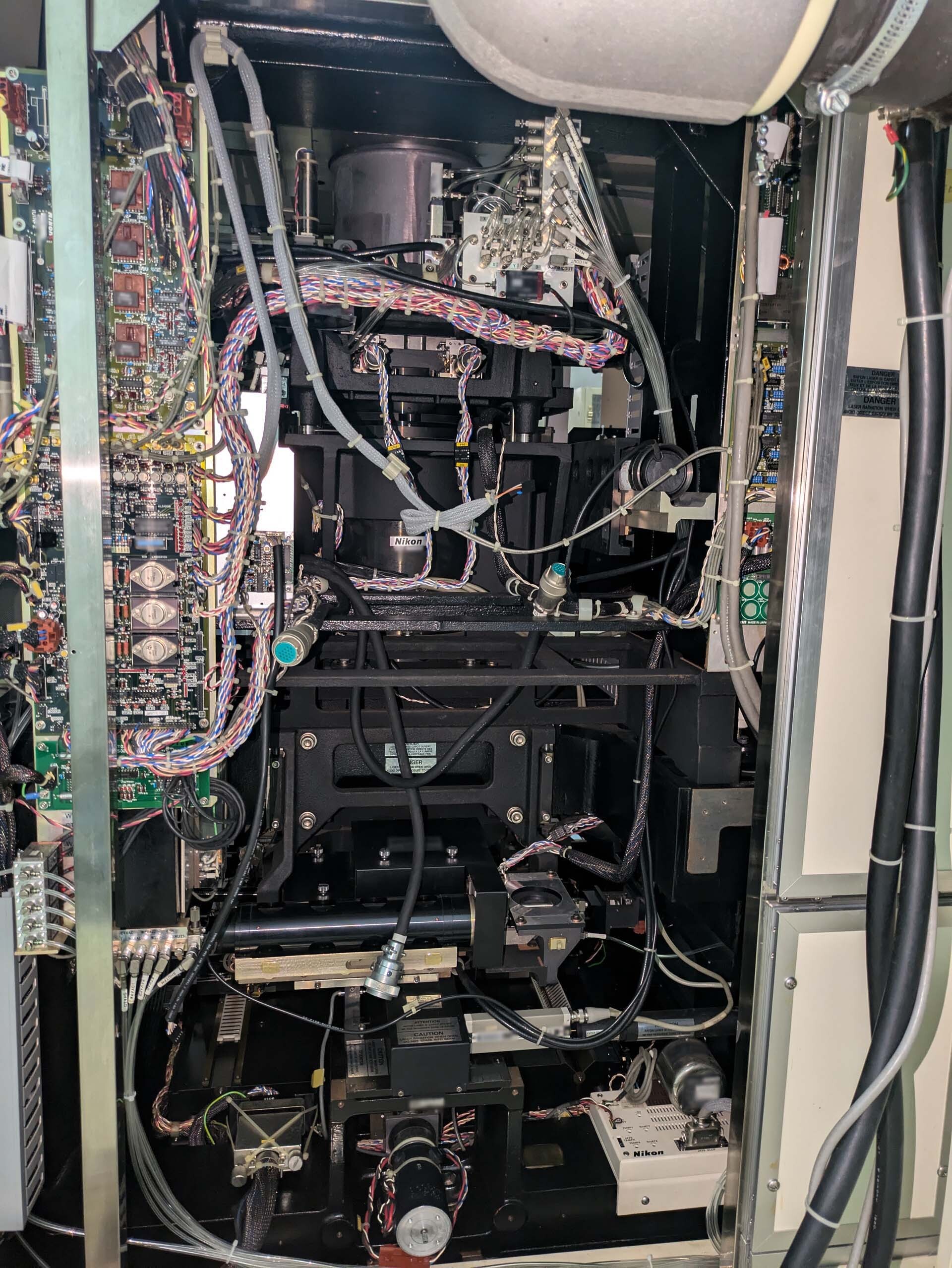
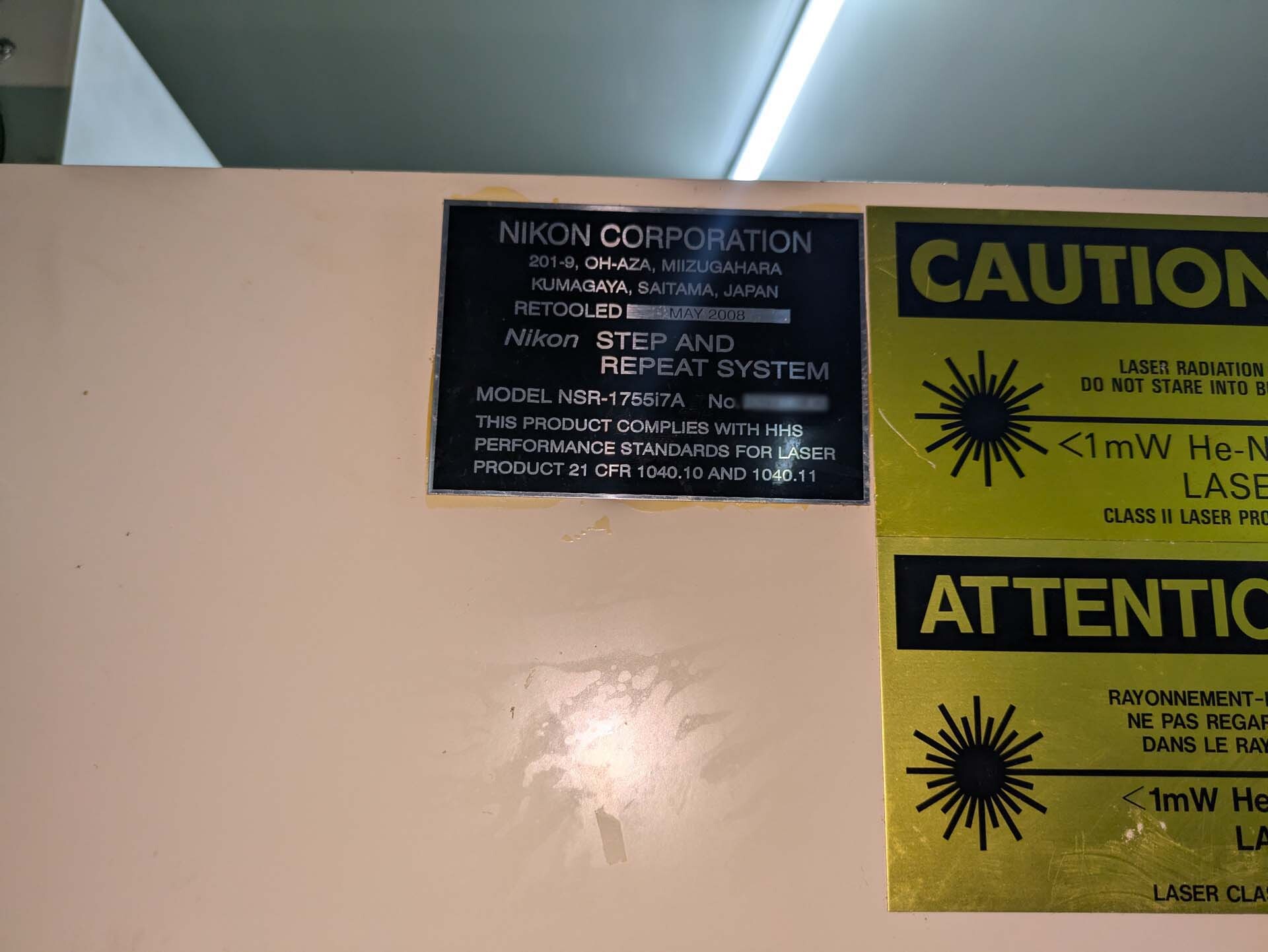
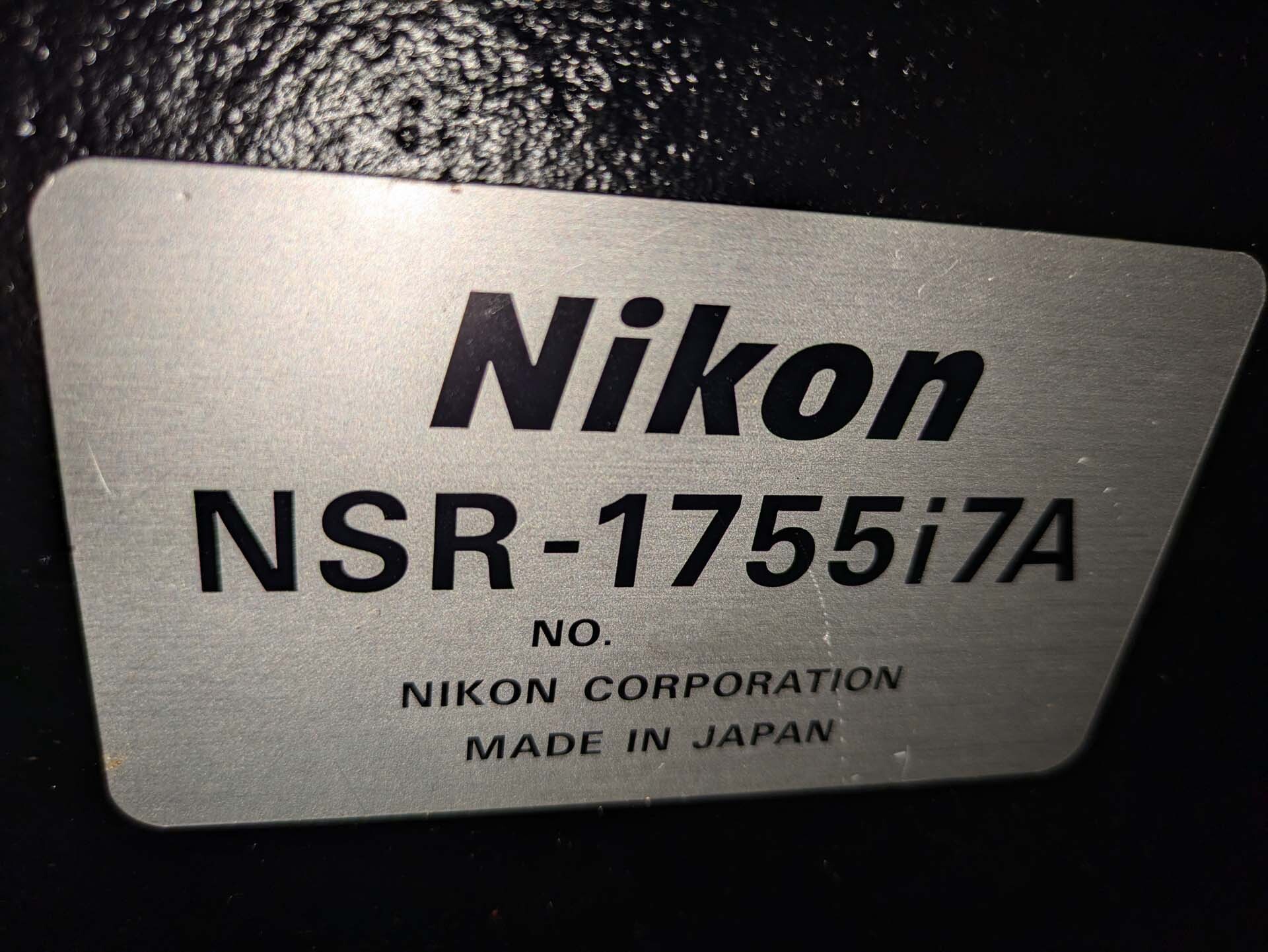
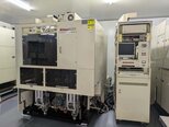
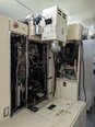
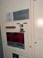
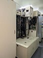
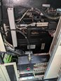
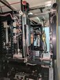
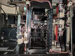
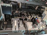
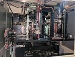
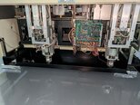
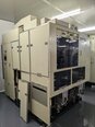
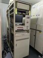
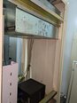
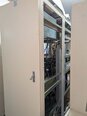
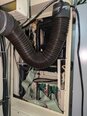
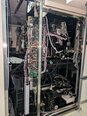
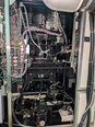
NIKON NSR 1755 i7A Wafer Stepper is a high resolution lithography equipment designed for printing advanced semiconductor chips with single-digit nanometer features. It utilizes cutting-edge optical technologies to enable imaging onto substrates up to 200mm in diameter, capable of delivering 12K and 15K resolution with high overlay accuracy. This precision system also features auto-calibration for quick and easy setup of different devices and a library of pre-defined functions for quick prototyping and process optimization. NIKON NSR 1755I7A Wafer Stepper utilizes an advanced optical unit to achieve the highest resolution and accuracy of any of NIKON lithography systems. It features NIKON patented NIS-AEA lenses, which employ a proprietary emission wavelength of ArF light and advanced all-reflective imaging optics to enable high resolution imaging in single-digit nanometers. It is also designed with modified and multi-focus optics with dual-axis auto-alignment capabilities to ensure high overlay accuracy. The machine also features NIKON HD-FSC, an algorithm with auto-calibration that allows the user to quickly and easily set up different devices for imaging and testing different processes and settings. In addition, its library of pre-defined functions allows users to quickly create, test, and optimize their processes with greater speed and accuracy. With a maximum substrate size of 200mm, NSR-1755I7A Wafer Stepper can accommodate a wide variety of chip designs. It is capable of high precision operation that meets design and production requirements for advanced semiconductor chips, while also delivering cost-efficiency. The tool also features an automated asset for process defect inspection, as well as automated job routing to optimize throughput and efficiency. NIKON NSR 1755 I 7 A Wafer Stepper is an advanced lithography model that combines cutting-edge optical technology with auto-calibration and pre-defined functions to enable ultra high resolution, high overlay accuracy, and improved cost-efficiency for semiconductor chips. It can accommodate substrates up to 200mm in diameter, and is capable of imaging single-digit nanometer features with 12K and 15K resolution. This precision equipment allows for quick and easy setup for different devices and process optimization with its library of pre-defined functions.
There are no reviews yet