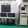
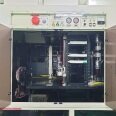
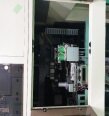
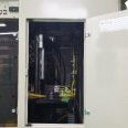
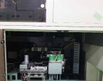
Used NIKON NSR 1755 i7B #9268107 for sale
URL successfully copied!
Tap to zoom


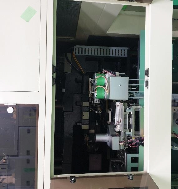

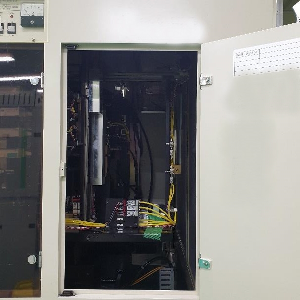

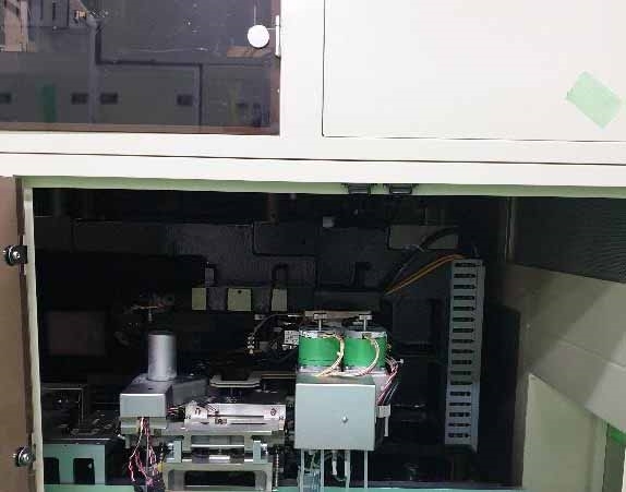

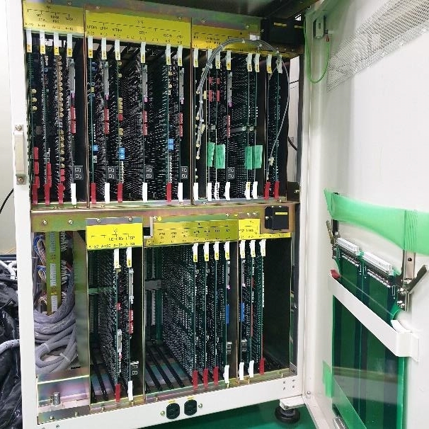

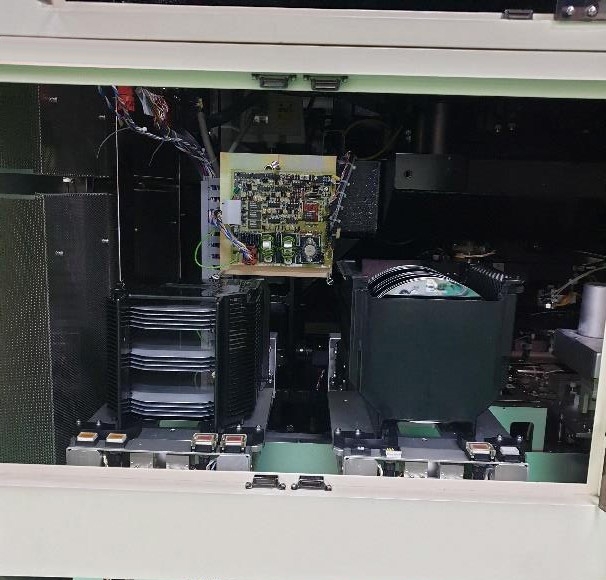

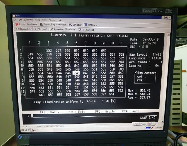

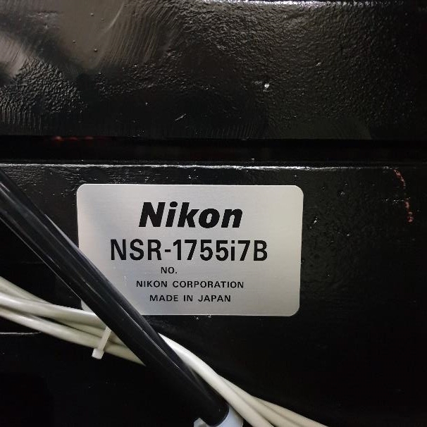

ID: 9268107
Wafer Size: 6"
Stepper, 6"
Flat wafer
ASAHI S78 Chamber
PLC Type: MELSEC F1-60 MR, F1-60 ER
Variable reticle microscope: 15 mm and 17.5 mm
AGILENT / HP / HEWLETT-PACKARD / KEYSIGHT 5517A Laser
LSA Laser: 5 mW
ITV Camera: RA CCD XC-77
Silicon wafer
OF Sensor: NIKON
UD Motor: 5.44:1
Wafer loader type: Type 1
No in-line
Wafer carrier table: Left and right
FIA
Reticle, 5"
Reticle case: 26 mm
(13) Reticle slots
No PPD / PD
Rack type: Right
Chamber temperature:
Chamber: 23°C
LATC: 22.6°C
Power: 200 V, 3-Phase, 4 Wires, 75 Amps.
NIKON NSR 1755 i7B is a state-of-the-art wafer stepper designed to offer exceptionally accurate photolithography for semiconductor device fabrication. This model features an advanced electron beam lithography (EBL) system enabling superior feature resolutions down to 0.01 μm. It is equipped with a heavy frame structure for accurate stage alignment and incorporates the latest NIKON Scan Angle Control (NSC) technology for improved wafer positional accuracy. Additionally, NIKON NSR-1755I7B wafer stepper is able to achieve direct-down-to-substrate patterning with an unmatched acquisition speed of up to 1.0 sec/die - eliminating the need for lengthy exposure times. The advanced EBL system also offers unbeatable resolution, high speed scanning and excellent stage alignment accuracy. This model includes a high throughput, large area scanner, and a unique high voltage optics system for fast scanning and optimized pattern overlay. The high speed communication between the EBL control unit and NSR 1755 i7B wafer stepper allows the operator to accurately control multiple process steps, such as maintaining position during long exposures, adjusting scan speed and size of the pattern, and other wafer preprocessing settings. NSR-1755I7B wafer stepper also features advanced wafer clamping capabilities that allow for accurate adjustments and quick changes when challenged by different substrates. Its high-precision drive systems increase registration accuracy and stability over a wide range of operating conditions. The model also provides an automated alignment function with pattern translation and scale adjustments, and utilizes a unique edge detector to quickly locate the wafer under a microscope. Ultimately, NIKON NSR 1755 i7B wafer stepper provides industry-leading accuracy and throughput, making it an ideal choice for both large and small scale device fabrication. The model's fast-scanning capabilities, wide variety of lithography, and adjustable stage settings give it the flexibility to be used for a wide range of advanced device fabrication processes. Its user-friendly interface makes it easy to operate, while its superior pattern resolution and superior process performance make it the ideal choice for any wafer stepper application.
There are no reviews yet
