Used NIKON NSR 2005 i8A #9016445 for sale
It looks like this item has already been sold. Check similar products below or contact us and our experienced team will find it for you.
Tap to zoom


Sold
ID: 9016445
Wafer Size: 6"
Vintage: 1991
i-Line stepper, 6"
Wafer stage results of last PM:
Wafer holder flatness (Spec. < 2.5 μm): 1.3 μm (no leveling)
Y mirror travel (Spec. < 5 μm): -0.7 μm
Orthogonality (Spec. ≤ 0.96 μrad): 0.2 μrad
Stepping (Spec. 3σ≤ 70 nm): 3σ X: 27 nm, 3σ Y: 27 nm
Back-step (Spec. 3σ≤ 70 nm): 3σ X: 45 nm, 3σ Y: 36 nm
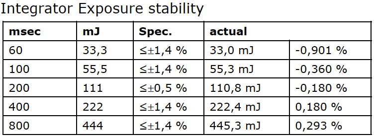
Illumination system results of last PM:
Lamp power: 447 mW/cm²
Uniformity (overall ≤ 1,5 %): 1.26 %
Actual vs. displayed power (≤±5 %): -3,712 %
Illumination tele-centricity (Spec. ±1 μm Z < 40 nm):
Xmax/min: 38/-17 nm
Ymax/min: 6/-32 nm
Lens results of last PM:
Lens inclination (Spec. Tilt ≤±0.2 μm)
UR-LL: 0.030 μm
UL-LR: 0.069 μm
Distortion (Spec. ≤±70 nm)
X max/min: 19/-32 nm
Y max/min: 47/-24 nm
Chamber:
Chamber front chamber temp: 23 ± 0.1 °C, 23.01
Pressure supply: 3 ± 0.1 Kg/cm², 3.1
Vac supply: > 460 mmHg, 650.00
Freeezer pressure:
High pressure: 15 ± 1 Kg/cm², 15.0
Low pressure: 4.85 ± 0.65 Kg/cm², 4.40
Wafer stage:
Clean and grease leadscrew X: OK, Y: OK
Clean and lubricate needle bearing X: OK, Y: OK
Perform stage running ca 10 min only after stage PM: OK
Check Interferometer mirrorsl X: OK, Y: OK
Check fiducial: OK
Wafer holder flatness (no leveling): 6" < 2,5 µm, max-min mm 2.2
Orthogonality: to customer wafer ≤ 0.5 µrad, Wafer_ORT= µrad 0.3
Stepping STEP spec: 3 sigma ≤ 70 nm, stepping 3 sigma X = nm 36
3 sigma Y = 27 nm
BACK spec: 3 sigma ≤ 70 nm, backstep 3 sigma X = 51 nm
3 sigma Y = 42 nm
Nikon i8 body:
Sr6c 5ib2
Sr lens 5ib2
Sr6b standard control rack
Sr6 accessory part 1
Sr6b lia
Sr6b lc 2
Sr6c iu 5ib2
Sr6c 5ib2 fe 5
Sr6c ws 8
Sr6 ceramic wh 5-8
Sr6c arl 56
Straight arm 5
Sr6c library adapter 5p 56
Sr6c wl 6 8
Sr6c wl extra carrier 68
Sr6c wa
Sr6c fia
Sr6c lia attachment part
Sr6c reticle table 5 6
Sr6c interferometer
Sr6c vacuum control
Sr6c pedestal
Sr6c avis
Sr6c control unit
Sr6c chamber s
Sr6c chamber panel 5 6
Sr6 lsa measurement software ver2.2
Sr6c ra 2 4 axis cameras mechanism 5
Sr6c aircondition 1b nema
Sr6 wl safety
Sr6b hg trap metal mesh
Sr6b rack modification us
Sr6 hg lamp outlet
Sr6c export tool
Sr6c laser safety part usa
Sr6c machine label
Sr6c safety label usa
Sr6c chamber label usa
Sr6c/8 high reflection board attachment parts
Sr 5ib2/c2 relay lens
Sr6 wafer cassette positioner if
Sr6c fia step 1
Sr6b/6c glass filter u-360
Sr6c extension cable protection cover
Sr6c ra2 cover for 4 axis camera
Sr6b hg lamp power supply ib2
Sr6c hg lamp power supply change ib5
Sr6c export mod ibm 973
Disassembled and crated
1991 vintage.
NIKON NSR 2005 i8A is a wafer stepper designed specifically for wafer level processing with integrated high throughput and high accuracy. The unit is capable of accommodating substrates up to 200 mm in diameter, allowing for a larger area than most conventional stepper systems. The precision optics equipment provides a high degree of accuracy and repeatability, allowing for a foundation of repeatable processes. Additionally, the integrated motion control and autofocus help minimize cycle time for improved throughput. The advanced alignment system of the unit features both coarse and fine alignment capabilities with a high level of accuracy and speed. The unit uses below field optics and high-resolution CCD cameras to precisely detect the exact position of each wafer after alignment. Further, the focus and alignment functions can be customized as needed to address specific substrate-level applications. The machine's illumination feature is highly customizable with a choice of wavelengths, numerical apertures and uniformity levels. This feature is essential for optimizing lithography results and ensuring the highest-quality images. Additionally, the unit integrates highly sensitive laser sensors and laser interferometry to measure the exact positions of each wafer, decreasing process variability and potential for errors. Additionally, the unit offers a large range of overlay compensation abilities and a variety of pattern recognition functions. This ensures that each wafer is accurately placed in the stepper without costly errors or rework, saving time and reducing costs. Further, a fully-automated main-load handling facility is available for hassle-free substrate loading, unloading, and changing. NIKON NSR 2005I8A comes equipped with a powerful, easy-to-use NIAS control interface that allows for complete process control. The intuitive graphical user interface allows for efficient process design, which increases throughput and helps reduce downtime. Additionally, the unit meets UL, CE, and FCC standards, meeting tightening safety and environmental regulations. Overall, NSR-2005I8A is a powerful and accurate wafer stepper designed specifically for medium- to high-volume wafer level processes. The unit features integrated high-precision optics, a highly customizable illumination tool, and automated main-load handling, allowing users to achieve fast, repeatable, and reliable results.
There are no reviews yet