Used NIKON NSR 210 #293820535 for sale
URL successfully copied!
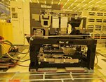
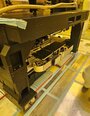
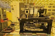
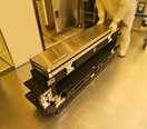
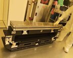
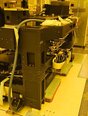
Tap to zoom
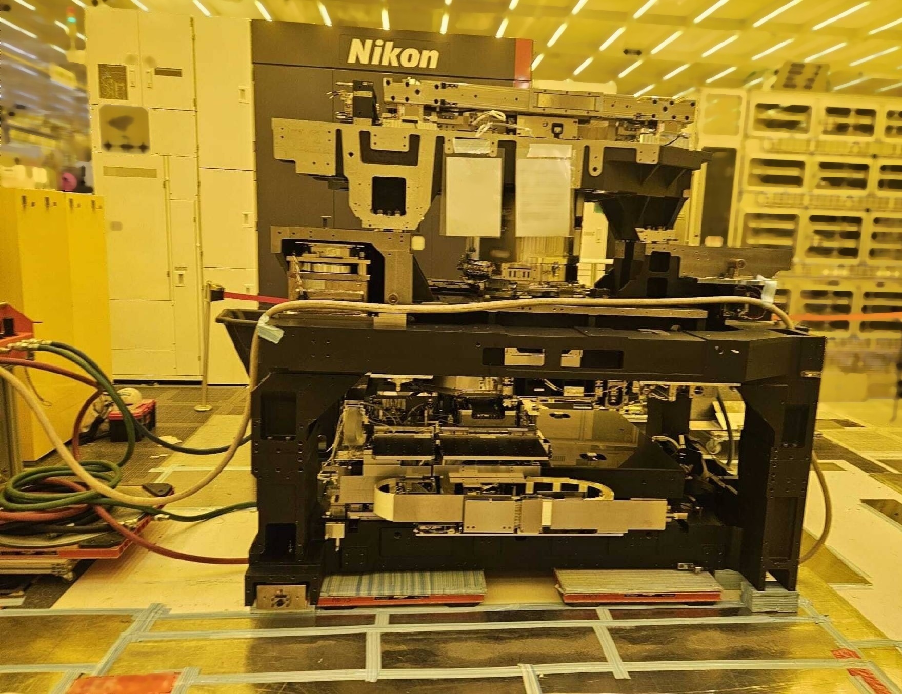

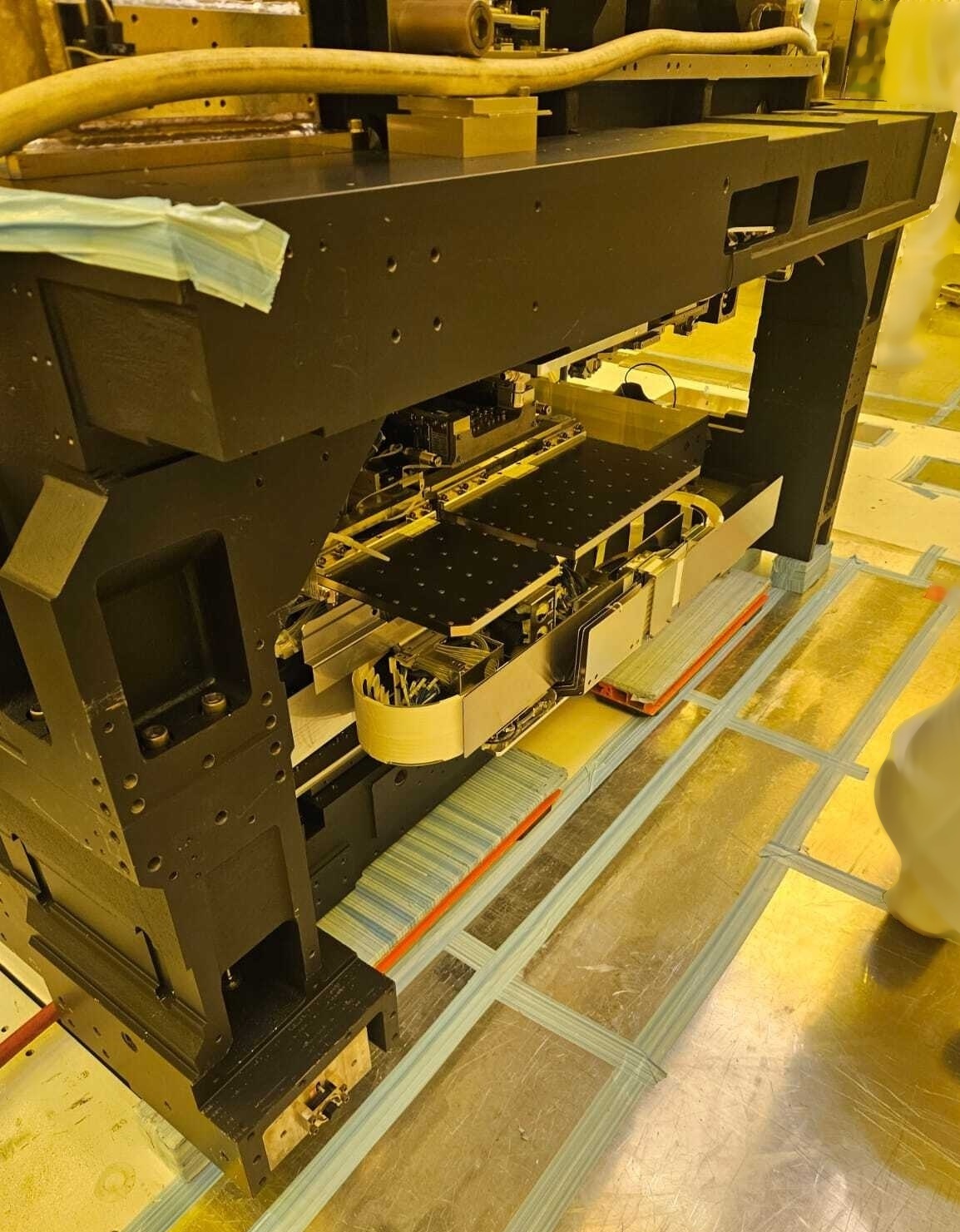
ID: 293820535
Wafer Size: 12"
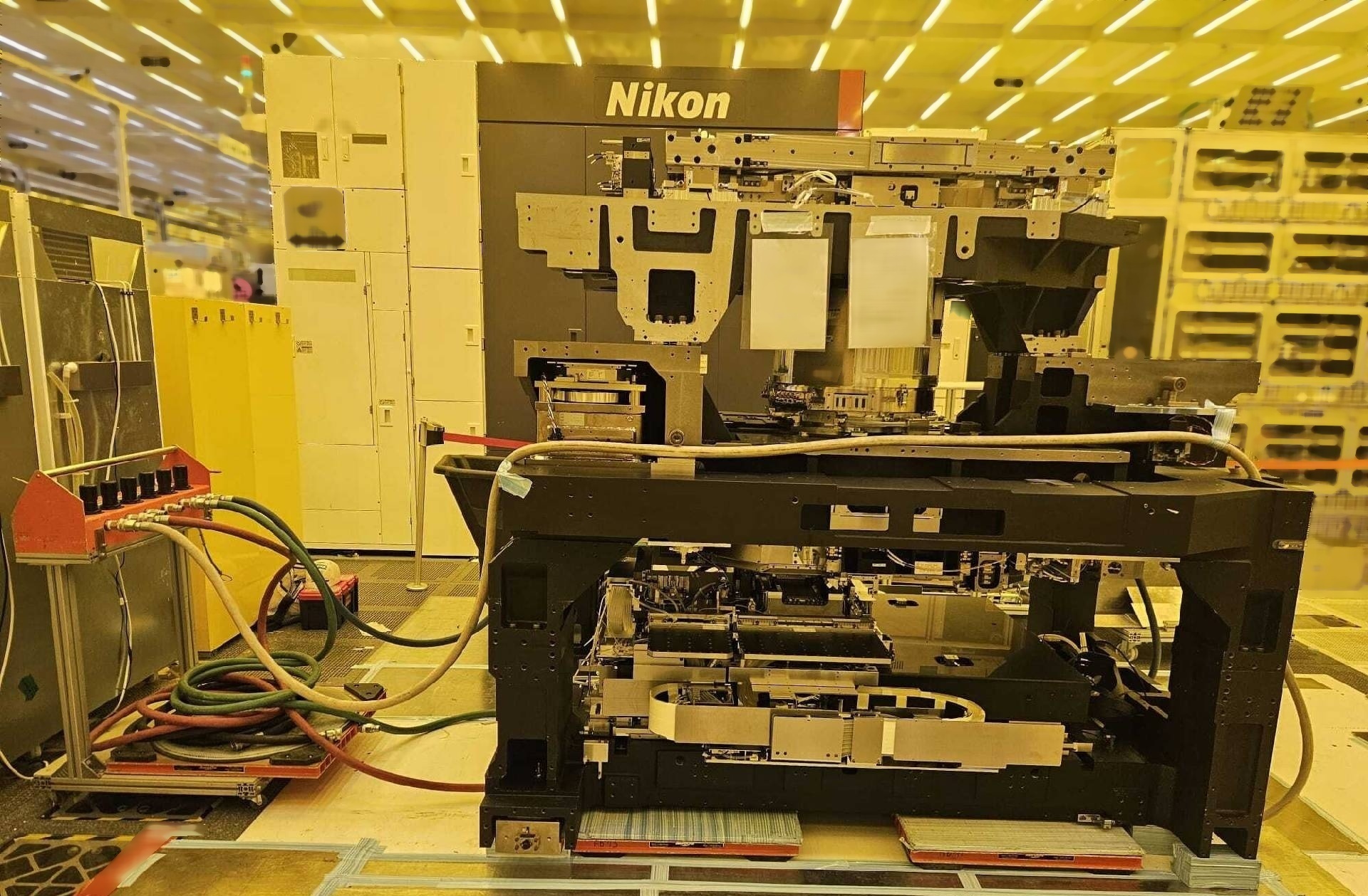
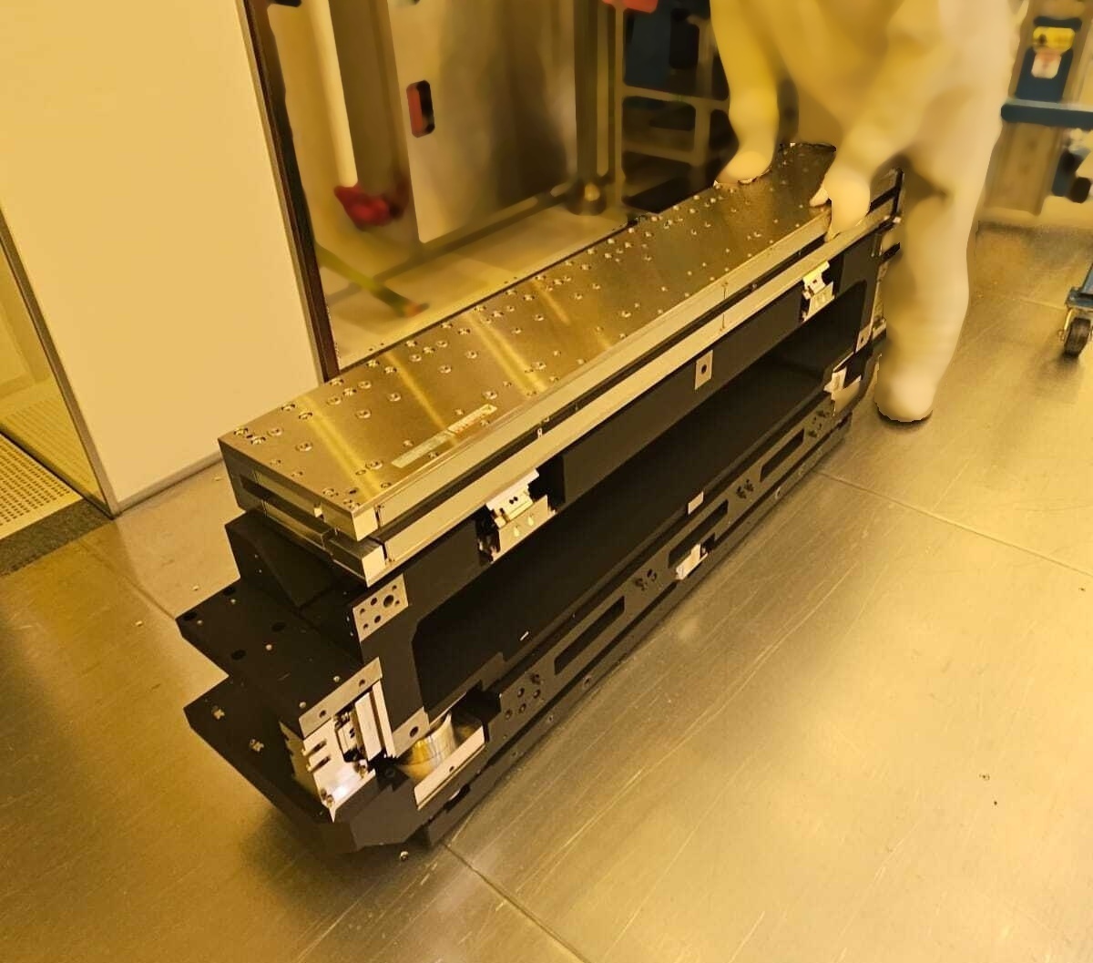
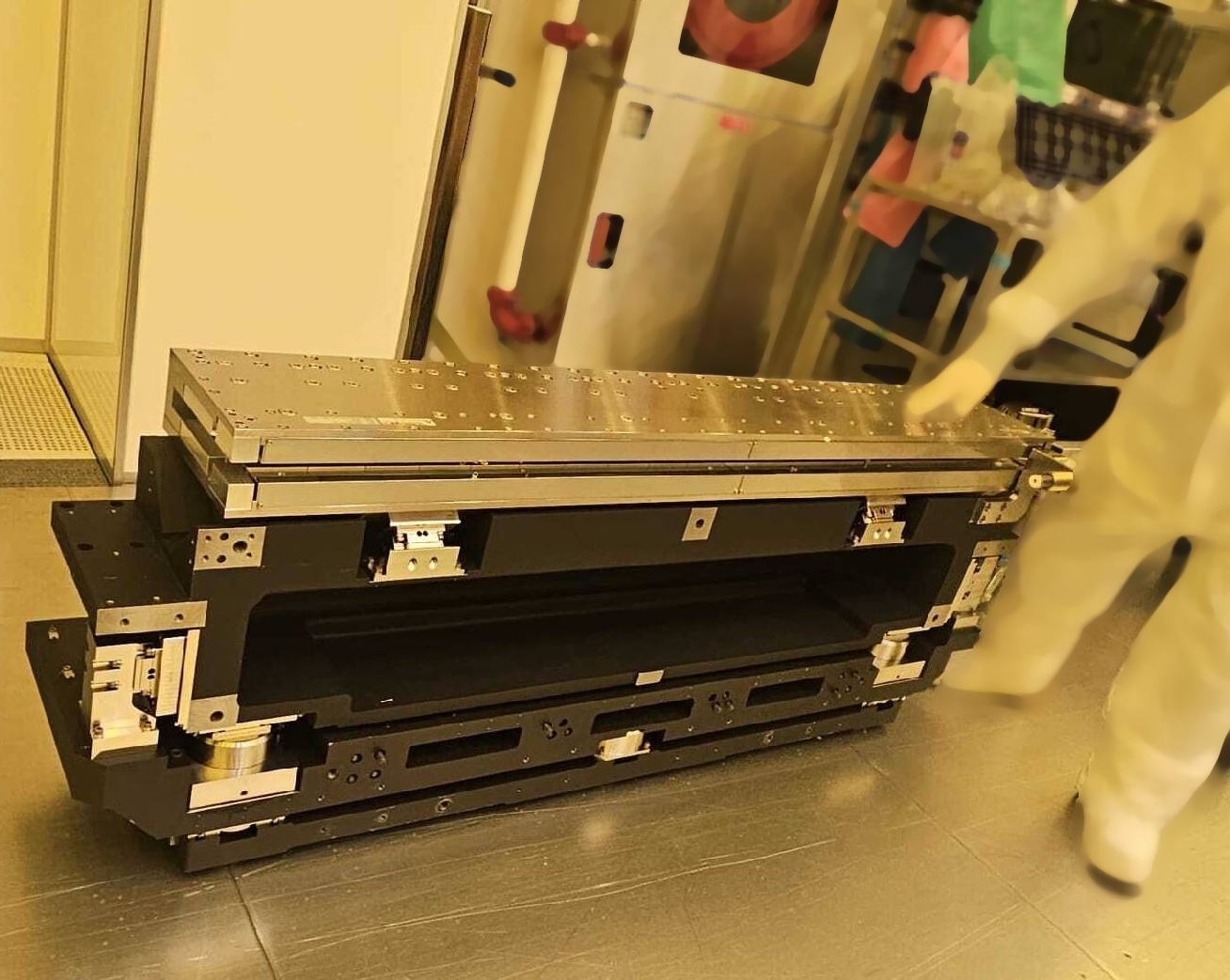
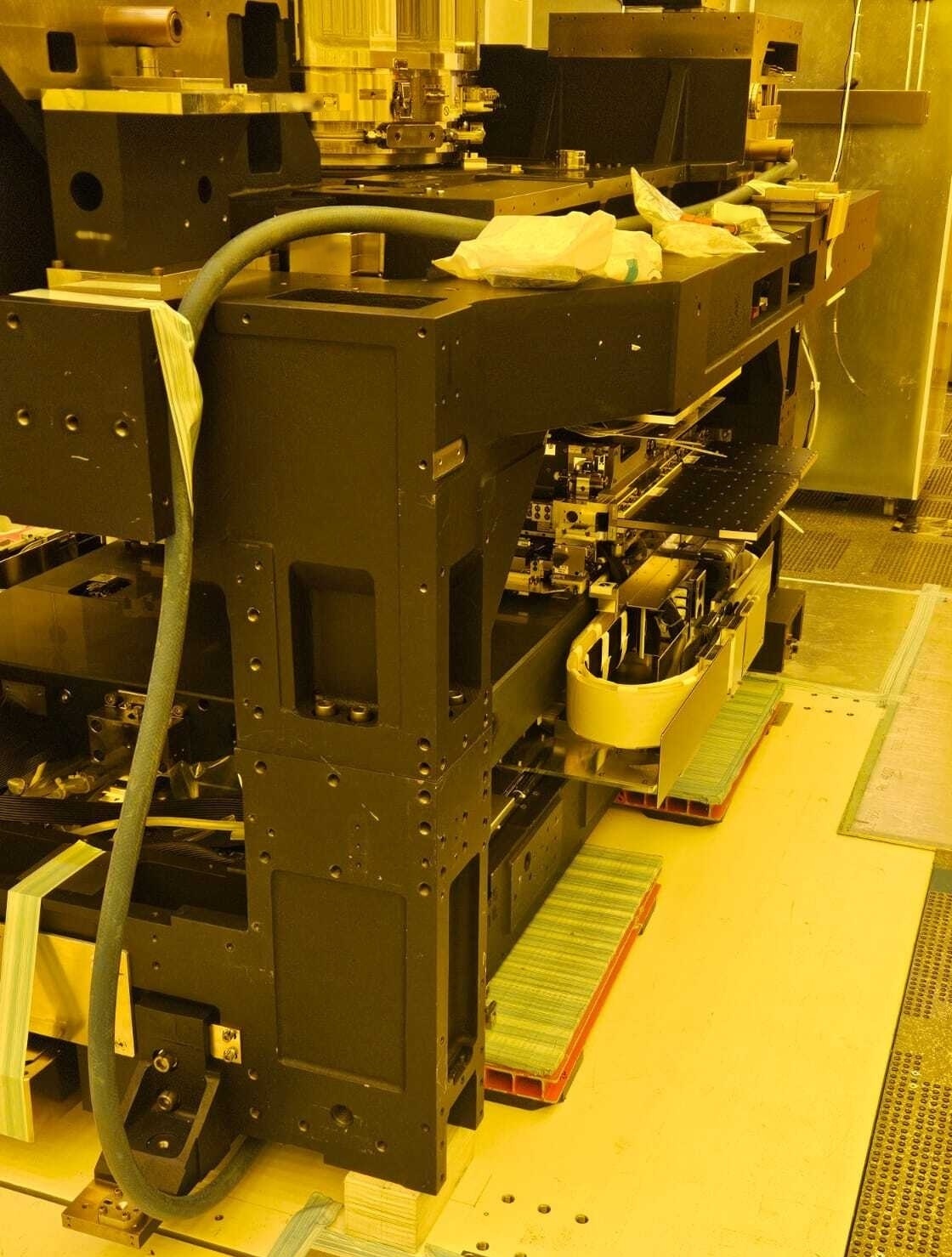
KrF Scanner, 12" parts system
Mainframe
Illuminator
(2) Wafer stages.
NIKON NSR 210 is a cutting-edge wafer stepper that is highly regarded in the semiconductor industry for its precision, efficiency, and advanced imaging capabilities. As a crucial tool in the semiconductor manufacturing process, NSR 210 plays a vital role in creating intricate patterns on silicon wafers with extreme accuracy and consistency. At the core of NIKON NSR 210 is its sophisticated optical equipment, which consists of a powerful light source, projection lens, and aligner. This optical system enables the wafer stepper to project intricate patterns onto the surface of a silicon wafer with ultra-high precision. The projection lens is a key component of the optical unit, as it is responsible for focusing the light onto the wafer with submicron-level accuracy. One of the standout features of NSR 210 is its advanced alignment capabilities. The wafer stepper is equipped with a high-precision aligner that ensures the accurate alignment of the wafer and the mask, which is crucial for creating precise patterns on the wafer surface. The aligner uses a combination of advanced algorithms and sensors to achieve submicron-level alignment accuracy, enabling NIKON NSR 210 to produce patterns with unmatched precision. In addition to its alignment capabilities, NSR 210 is also equipped with a state-of-the-art autofocus machine that ensures sharp and crisp imaging of the patterns on the wafer surface. The autofocus tool uses advanced algorithms and sensors to continuously adjust the focus of the projection lens during the exposure process, ensuring that the patterns are imaged with the highest level of clarity and detail. NIKON NSR 210 is also renowned for its exceptional throughput and efficiency. The wafer stepper is designed to process wafers at a high speed, allowing semiconductor manufacturers to achieve high levels of productivity and yield. NSR 210's robust design and advanced automation features streamline the wafer processing workflow, further enhancing its efficiency and throughput. Furthermore, NIKON NSR 210 is highly versatile and can accommodate a wide range of wafer sizes and substrates. The wafer stepper supports various exposure techniques, including proximity printing, contact printing, and projection printing, enabling semiconductor manufacturers to choose the most suitable technique for their specific requirements. Overall, NSR 210 is a top-of-the-line wafer stepper that offers unparalleled precision, efficiency, and imaging capabilities. Its advanced optical asset, alignment capabilities, autofocus model, and throughput make it an indispensable tool for semiconductor manufacturing processes requiring high-precision patterning on silicon wafers. With its cutting-edge technology and robust design, NIKON NSR 210 sets a new standard for wafer steppers in the semiconductor industry.
There are no reviews yet