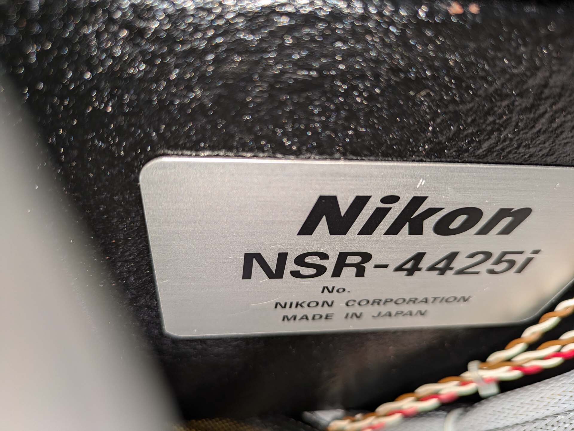
Used NIKON NSR 4425i #293719076 for sale
URL successfully copied!
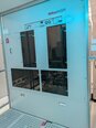

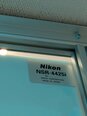
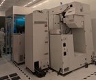
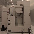
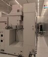
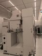
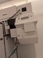
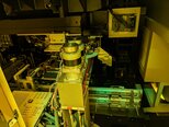
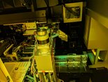
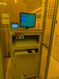
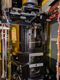
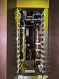




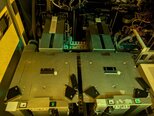
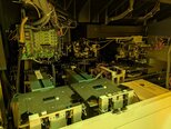


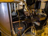
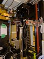
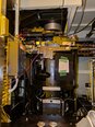
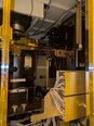
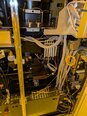
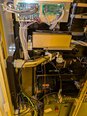



Tap to zoom
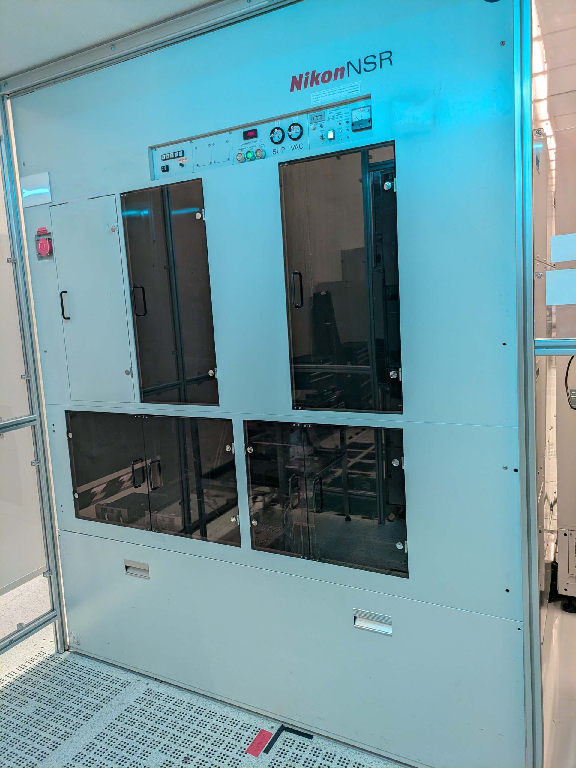

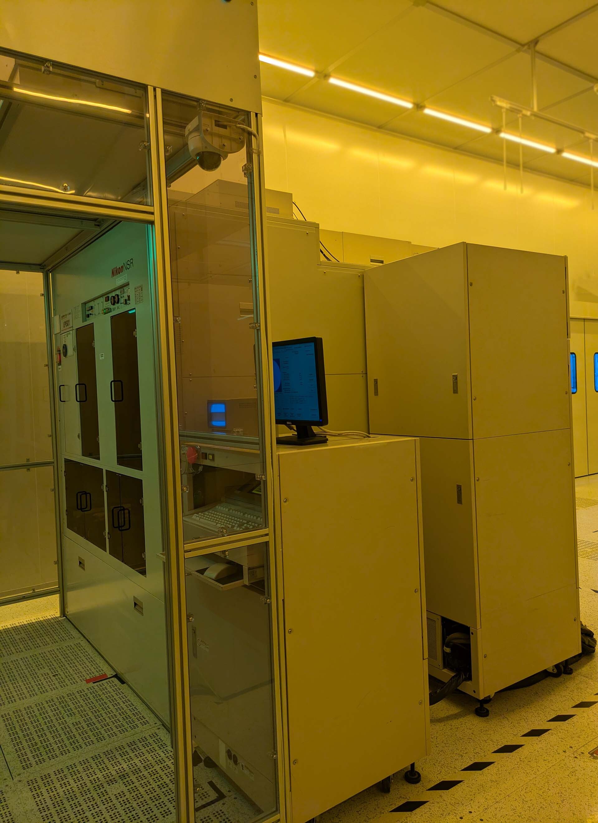
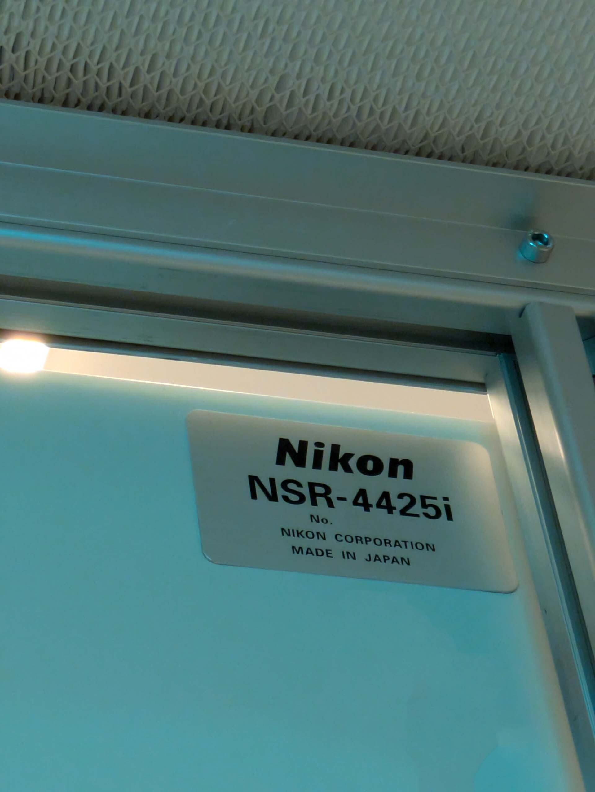
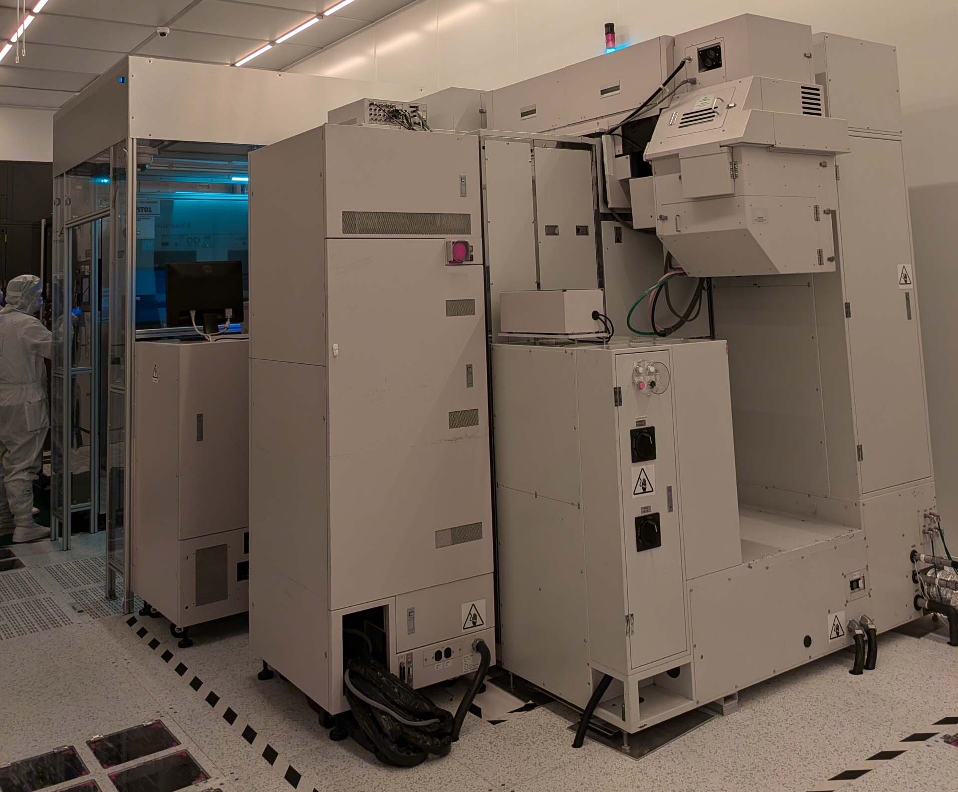
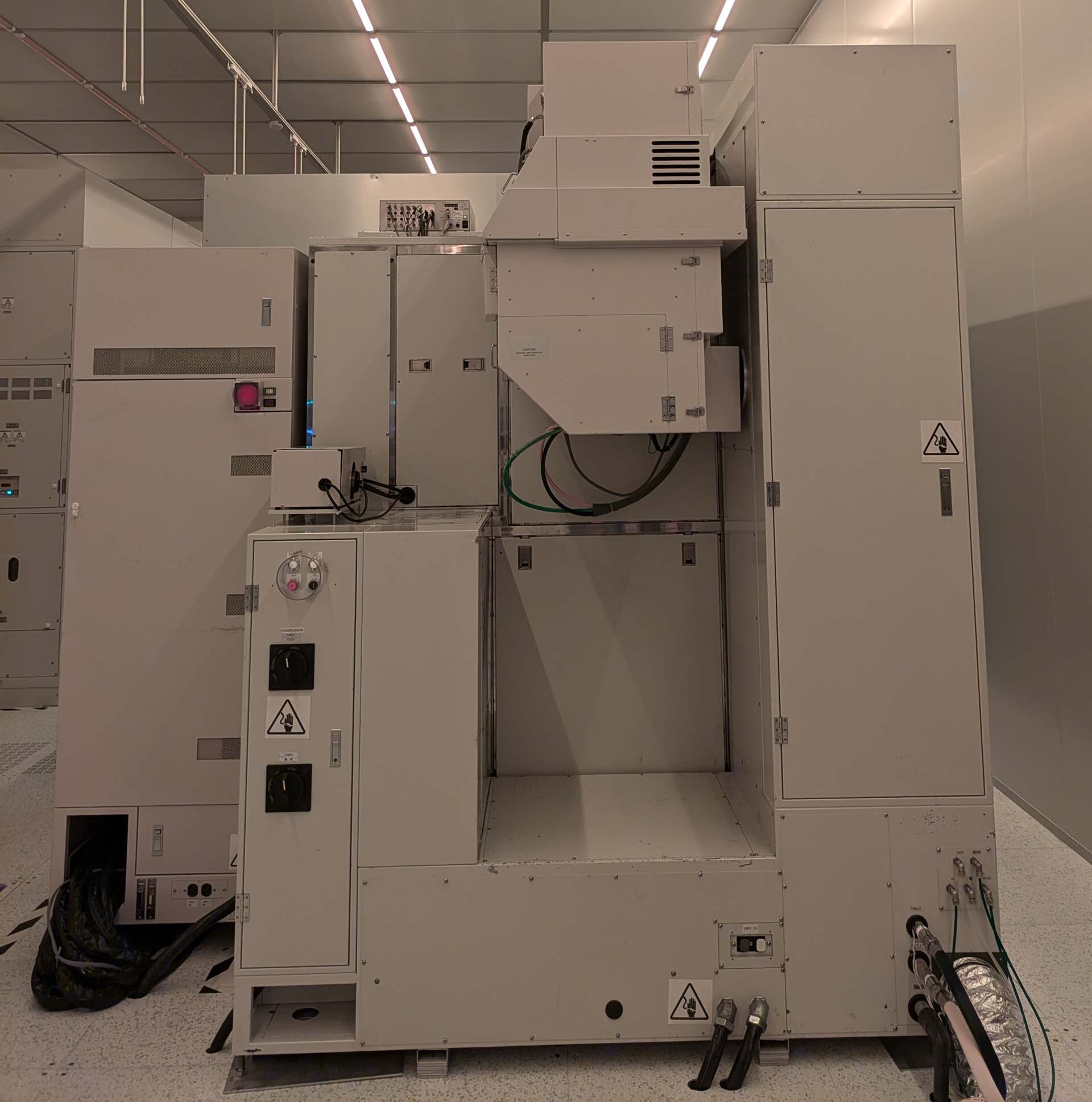
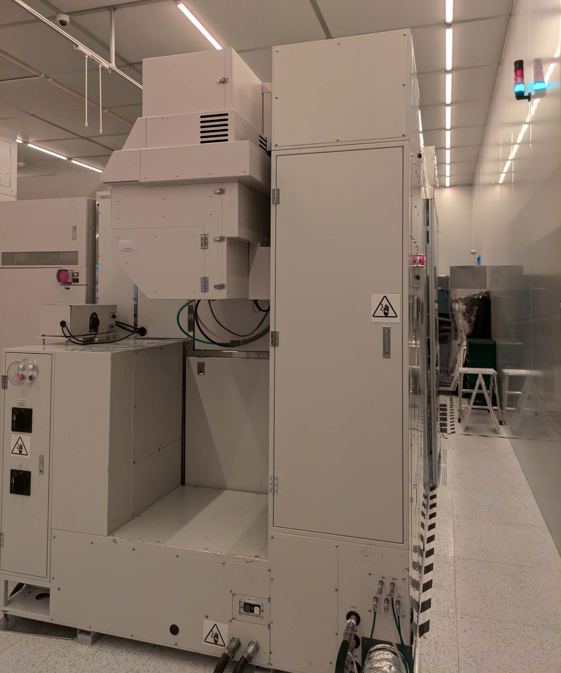
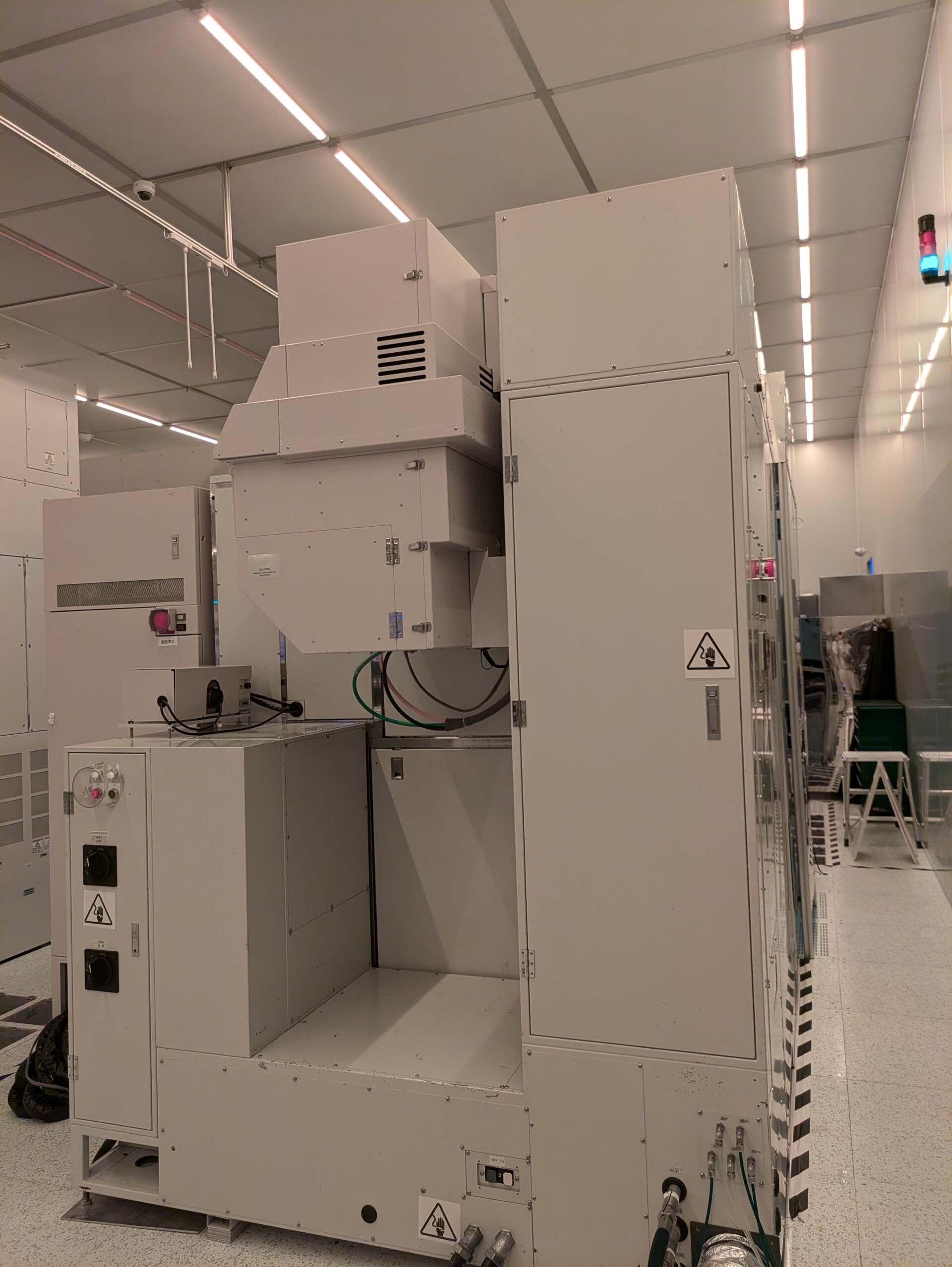
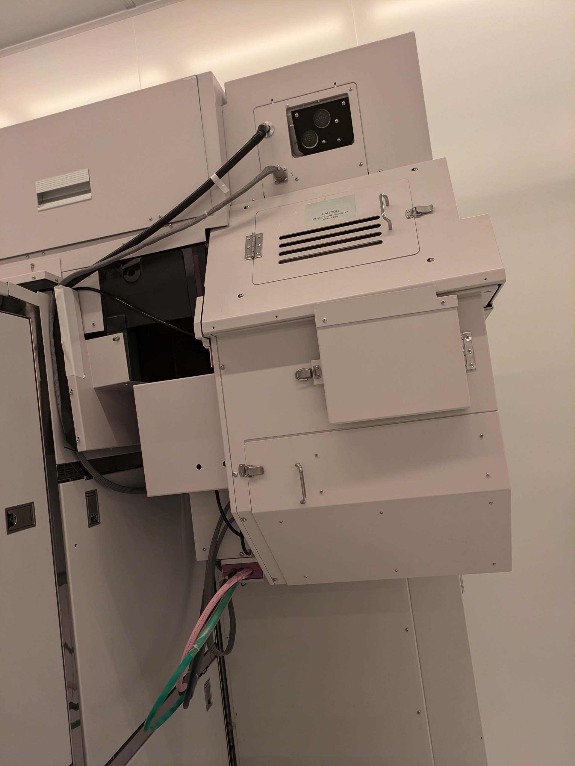
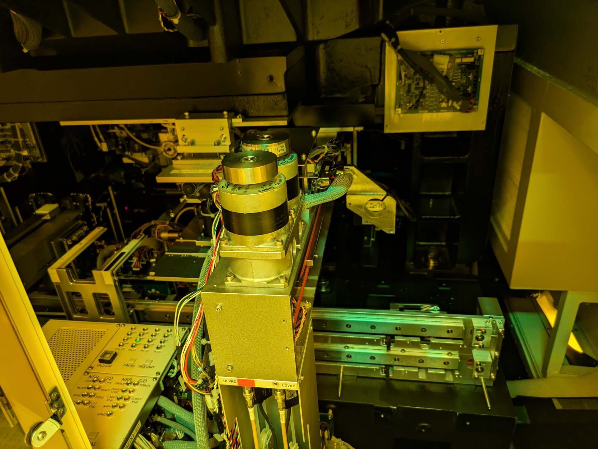
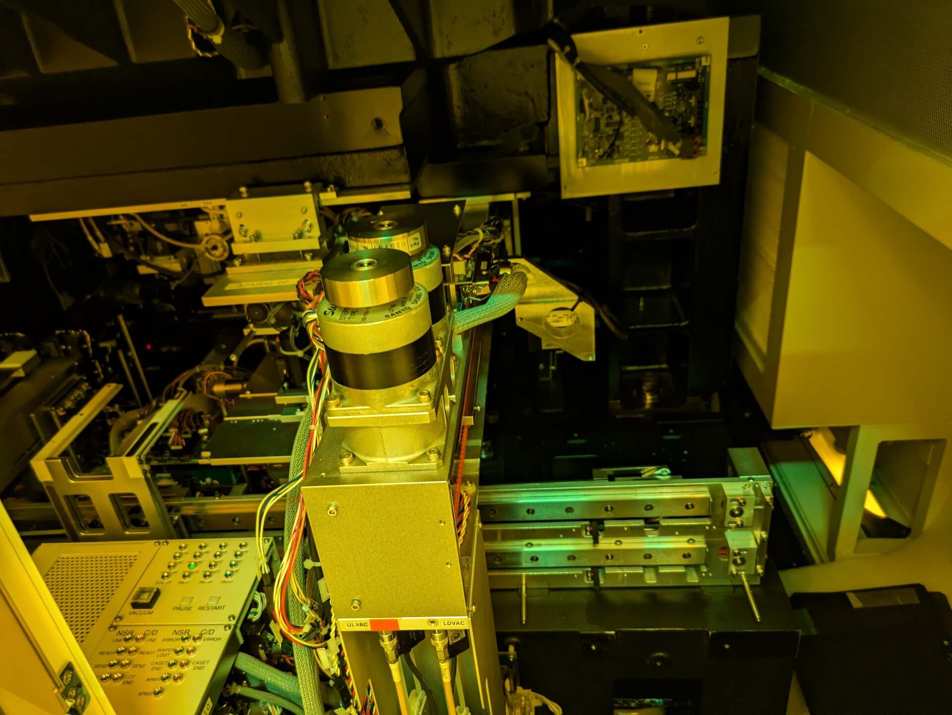
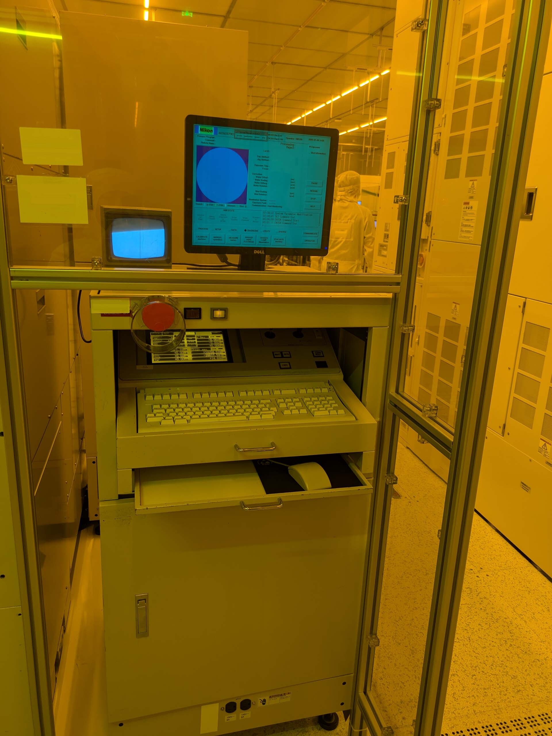
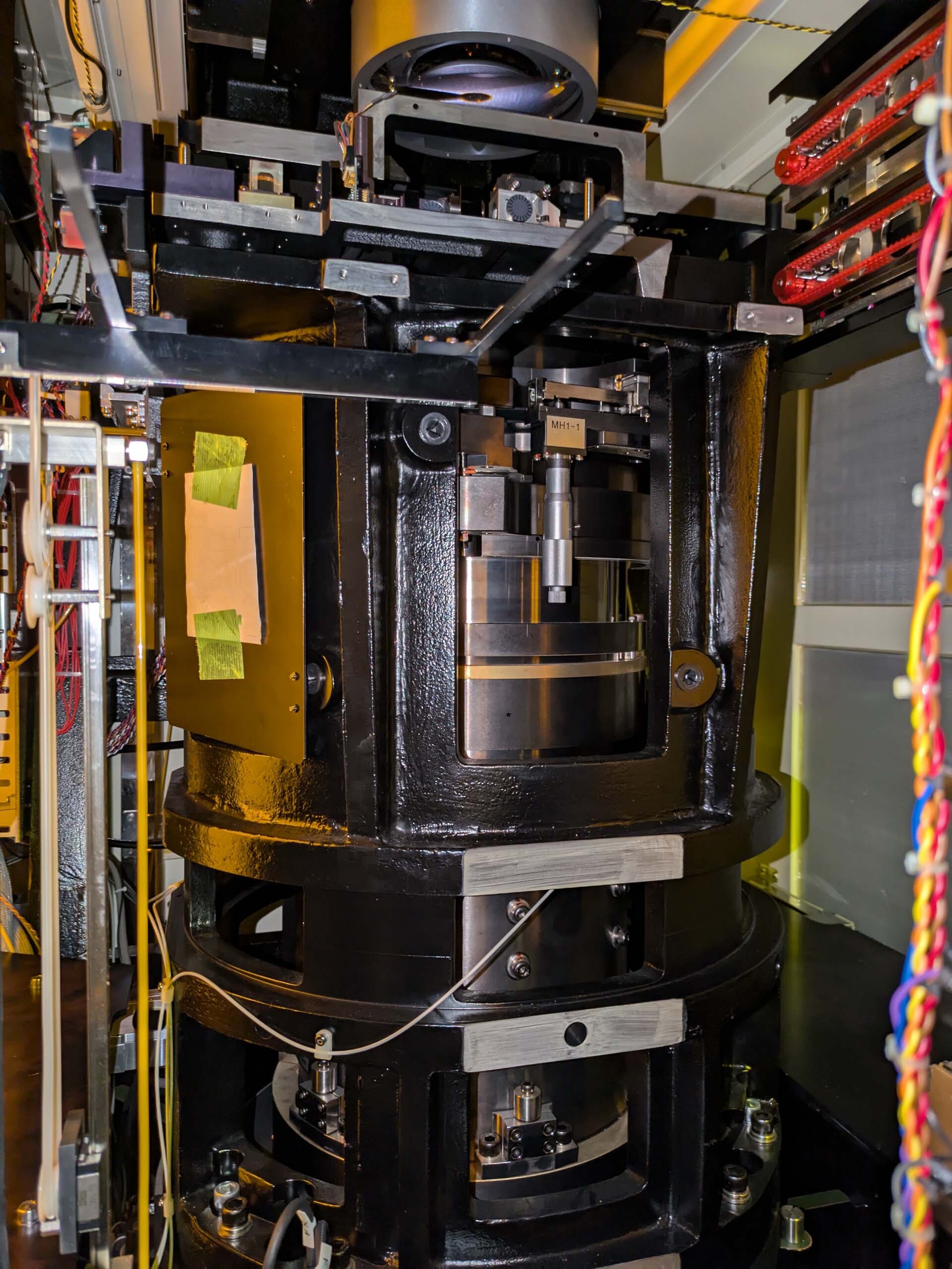
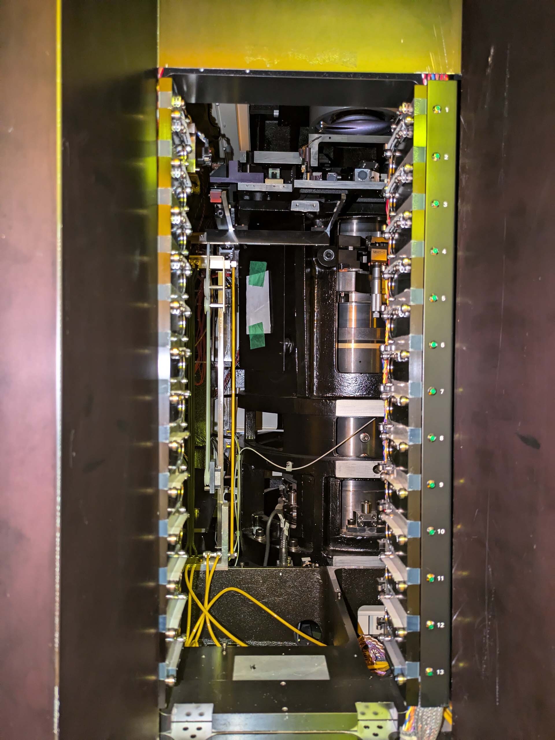
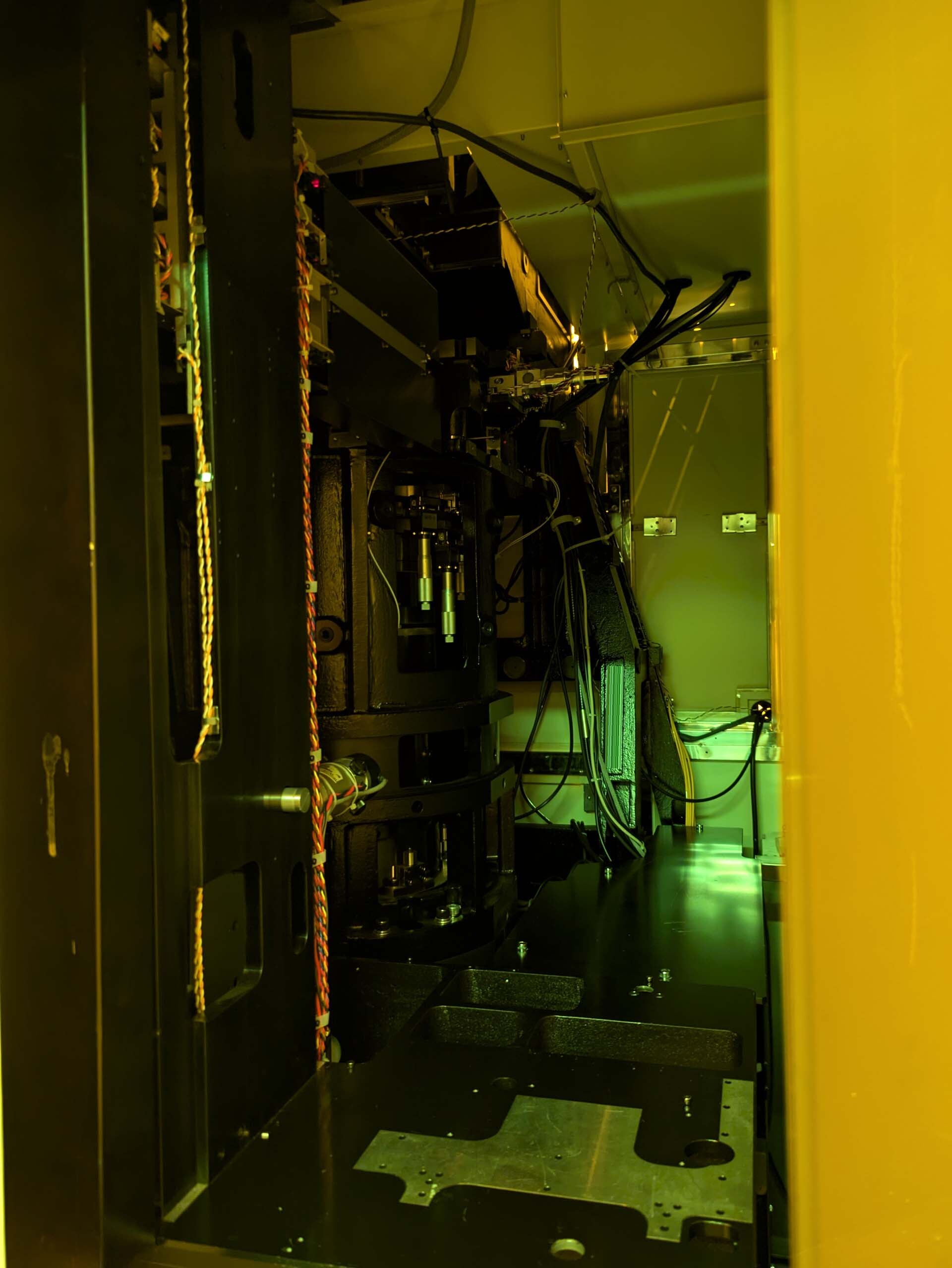
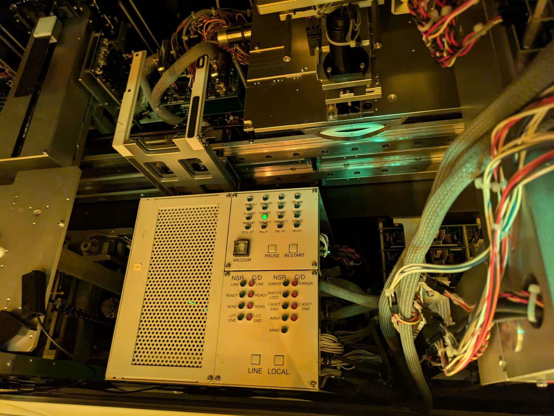
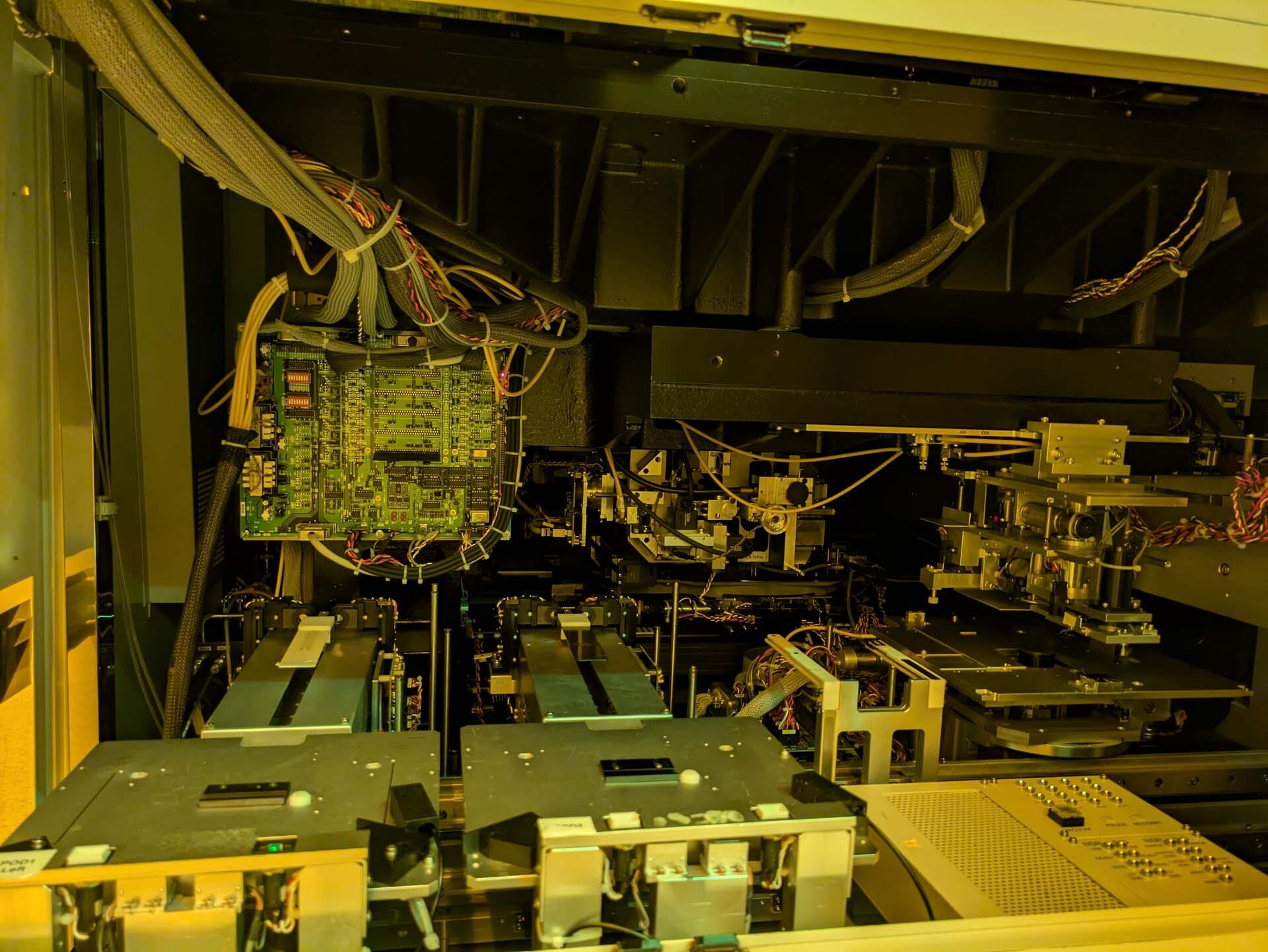
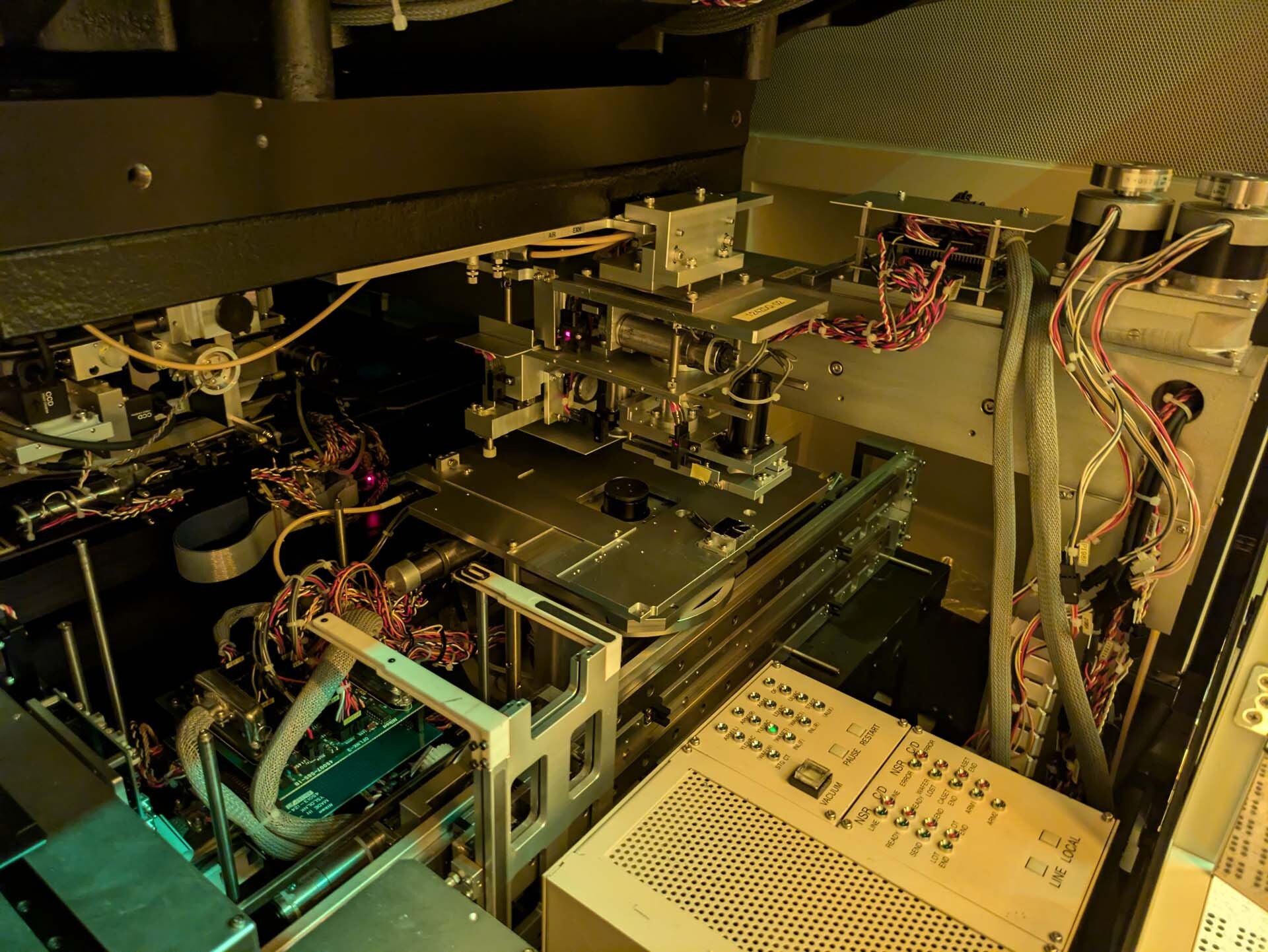
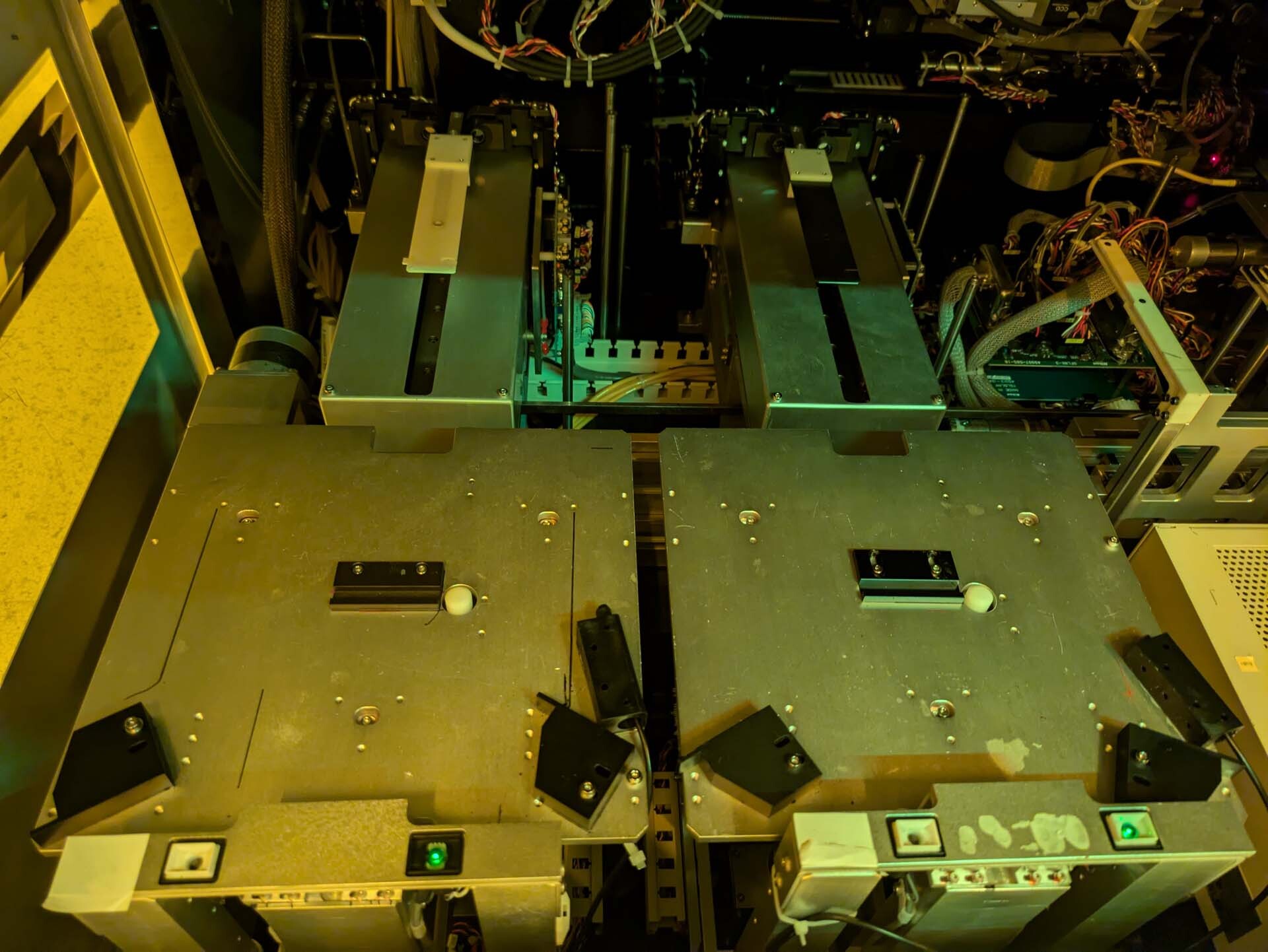
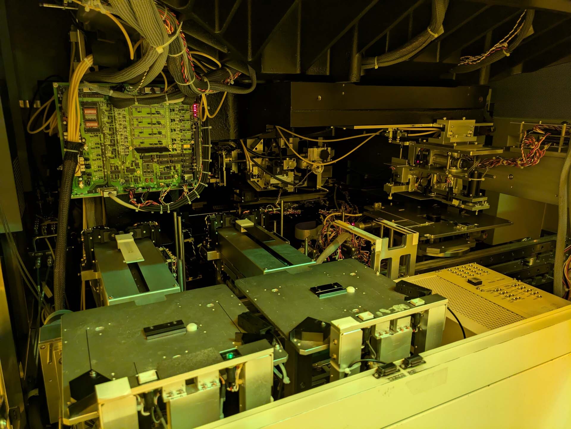
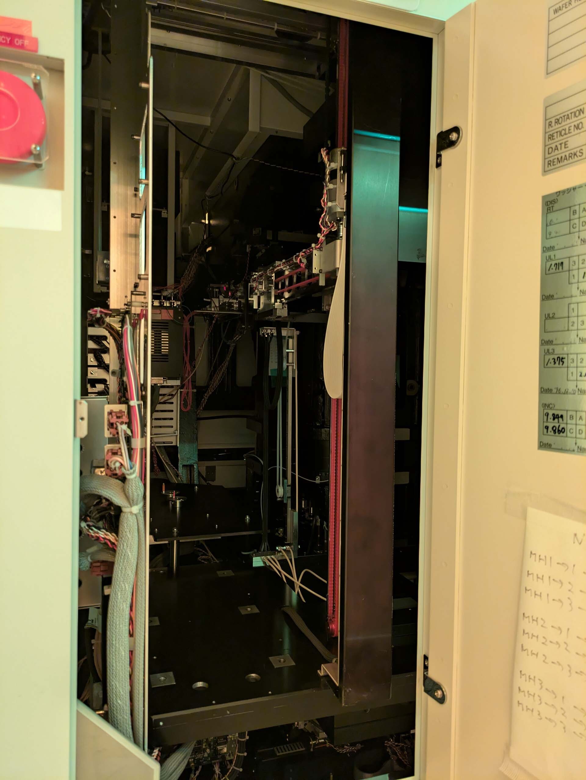
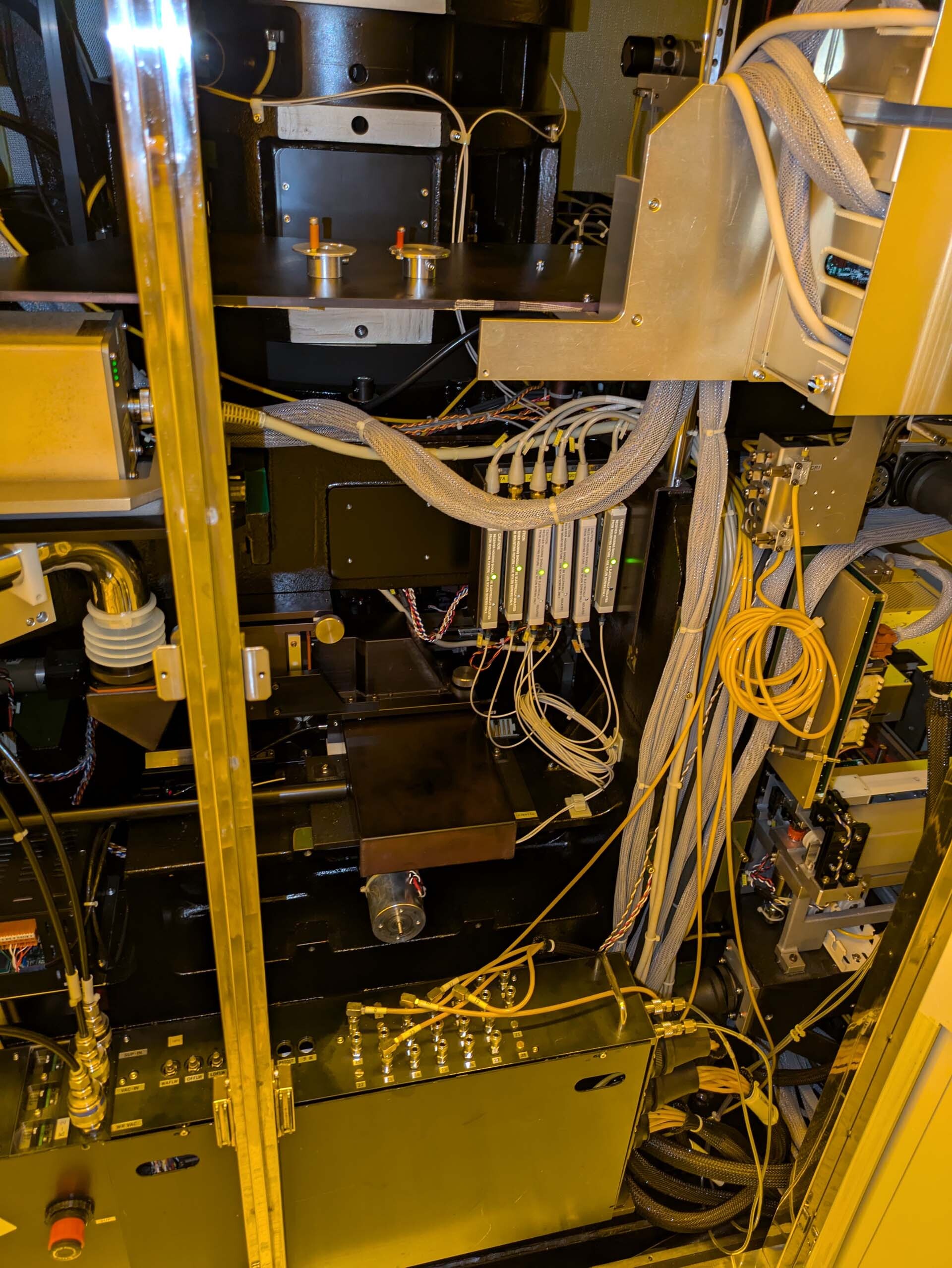
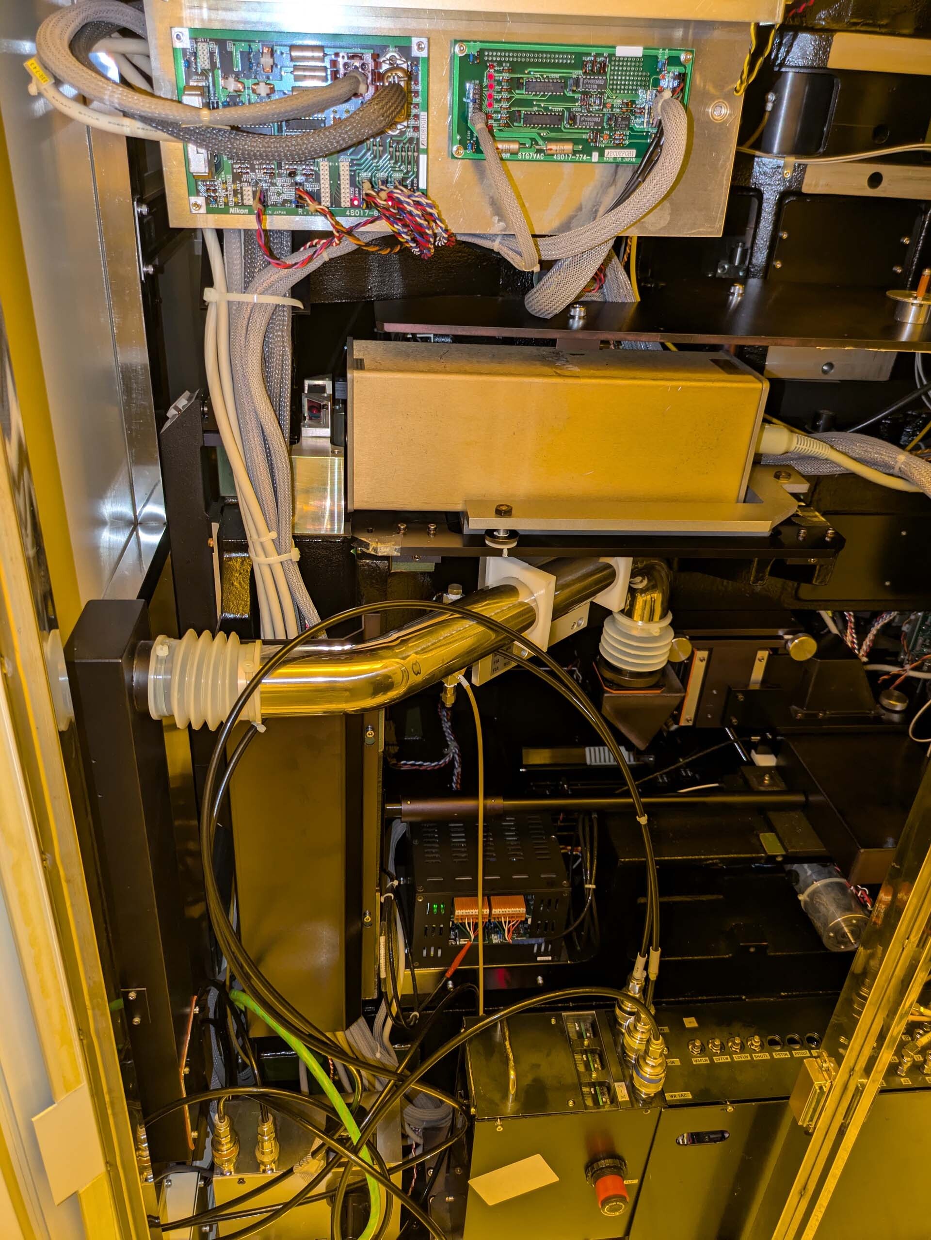
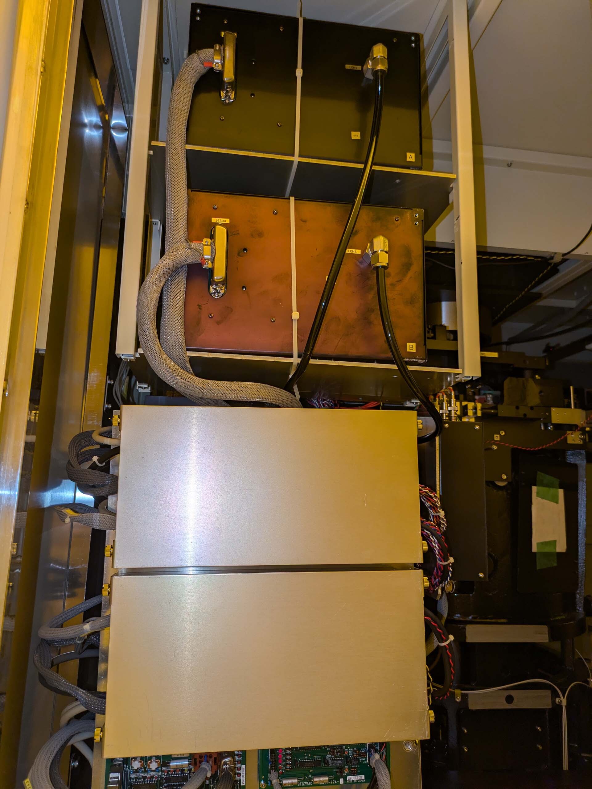
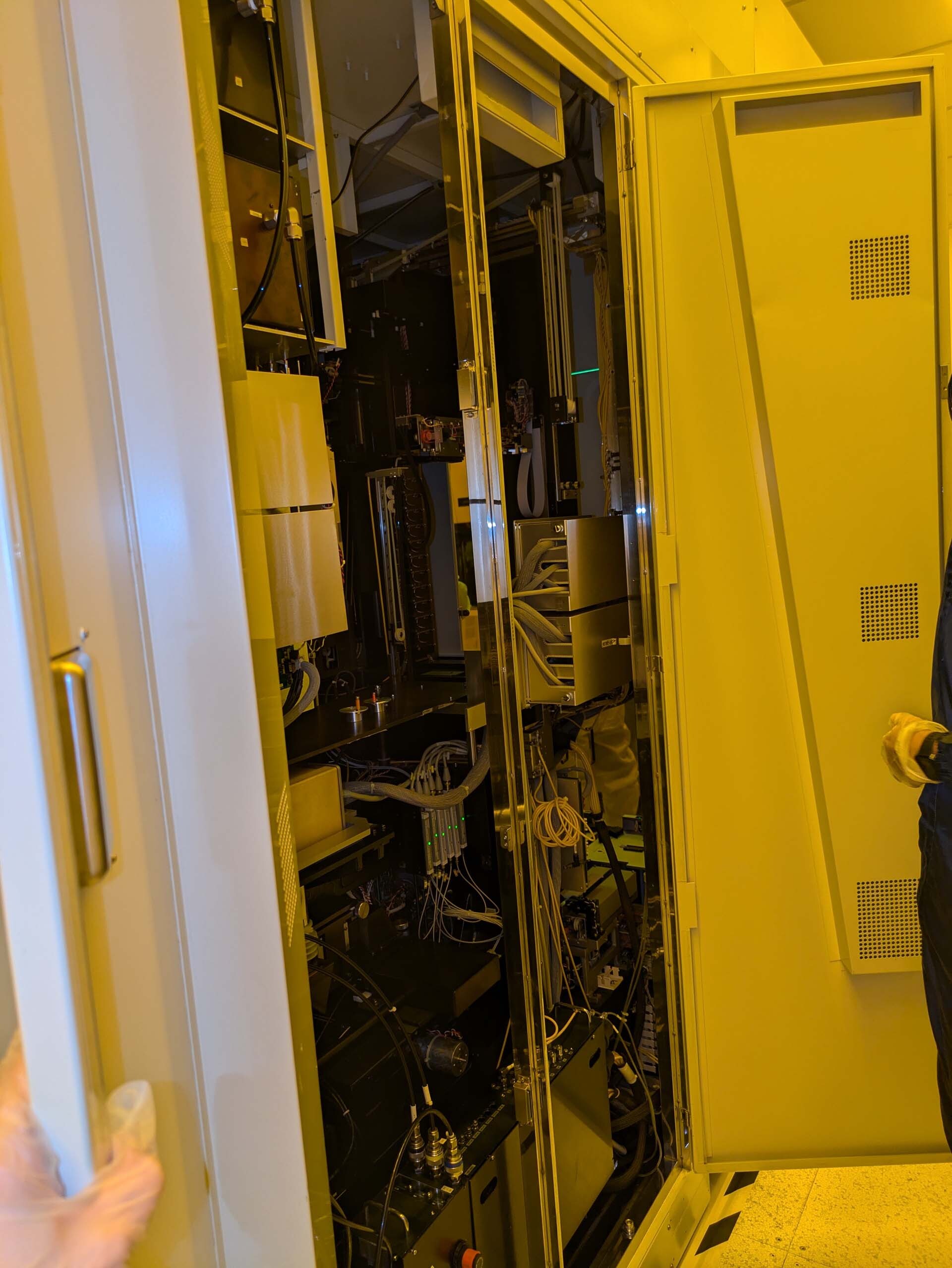
ID: 293719076
Wafer Size: 8"
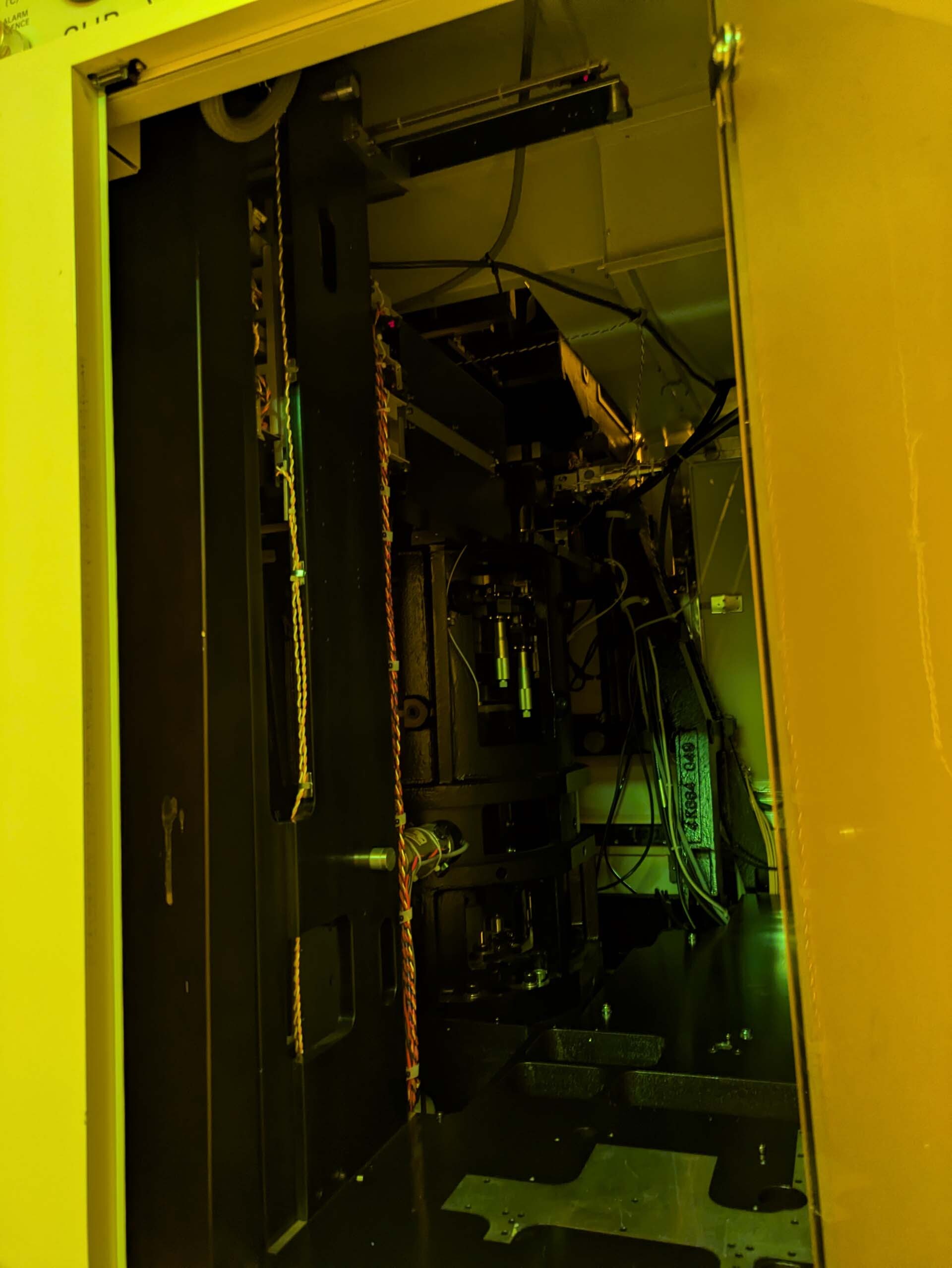
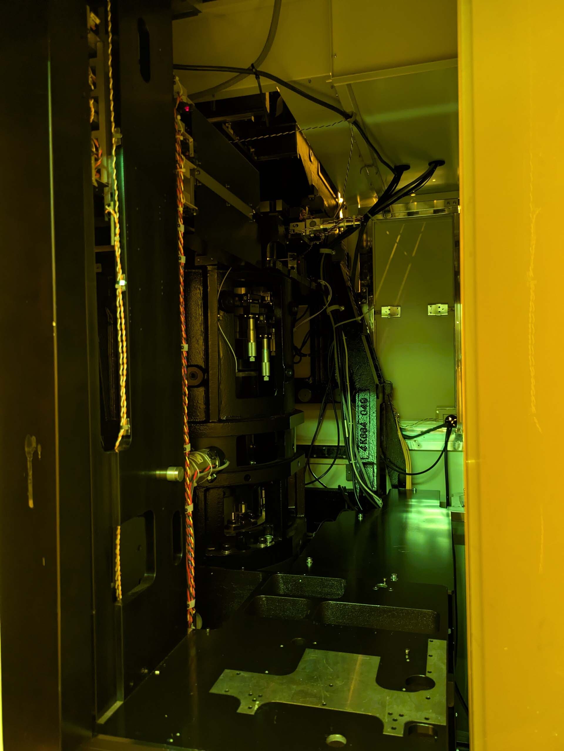
Stepper, 8"
Reticle loader
Reticle size, 6”
Field size: 44 mm x 54 mm
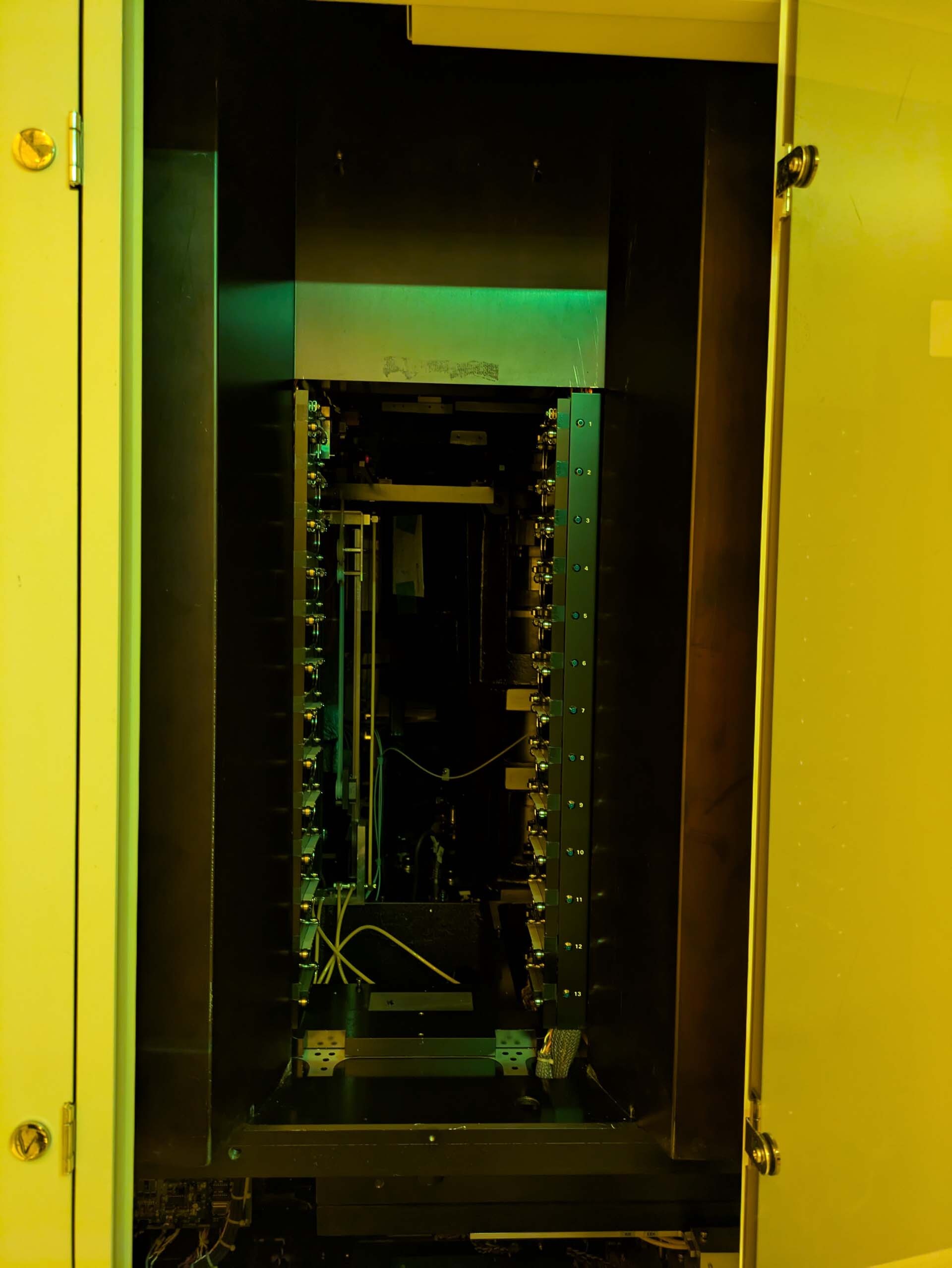
Library slot: 13
Wafer type: Notch
Wafer loader: Type 2
Wafer alignment: LSA, FIA and EGA
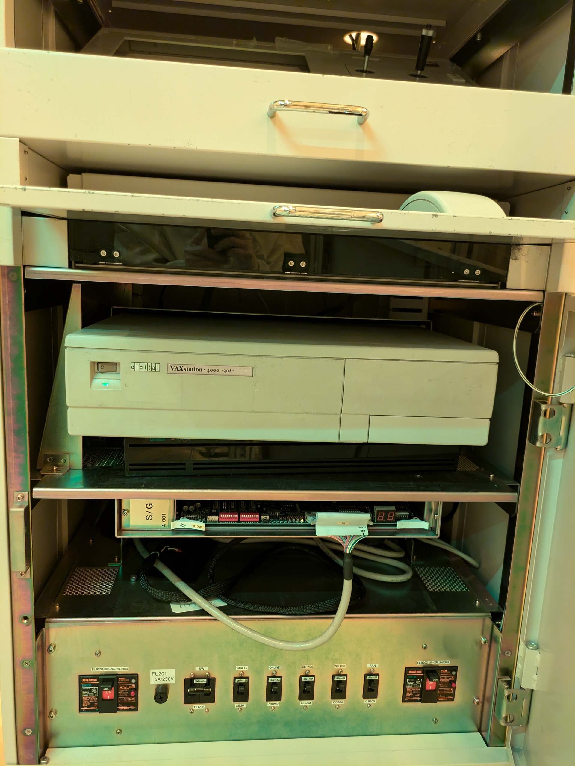
Disk drive: SSD / DOS
Ring chuck
WS-Ball screw
(2) Cassettes
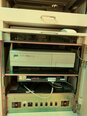
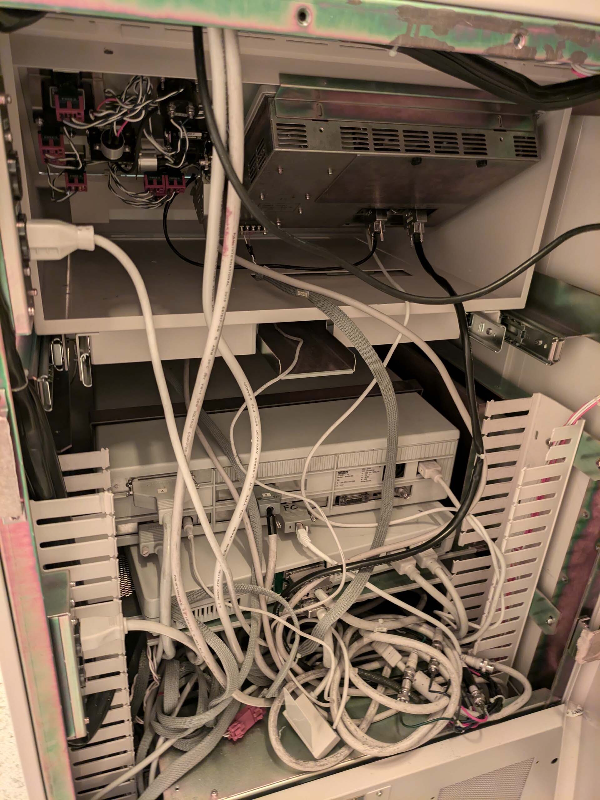
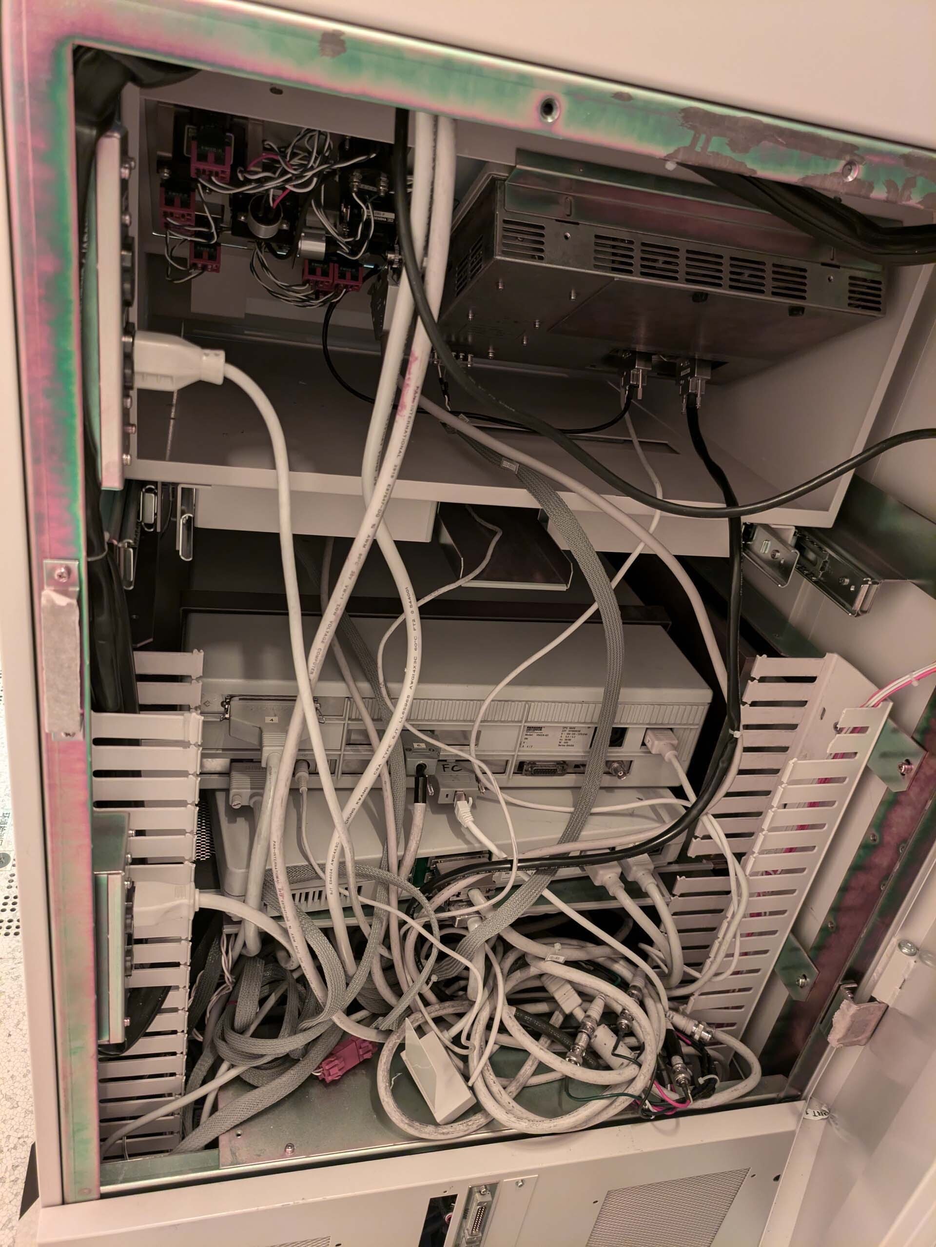
Control rack
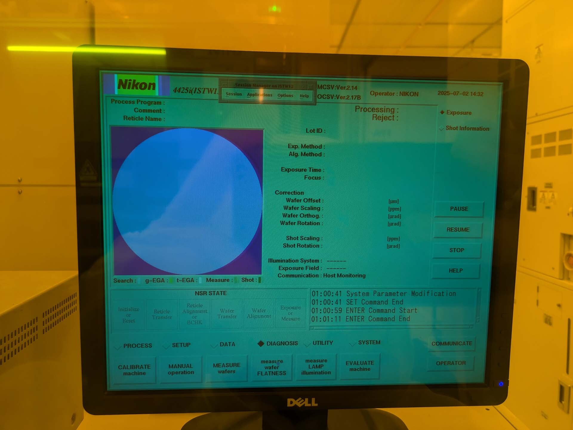
PC.
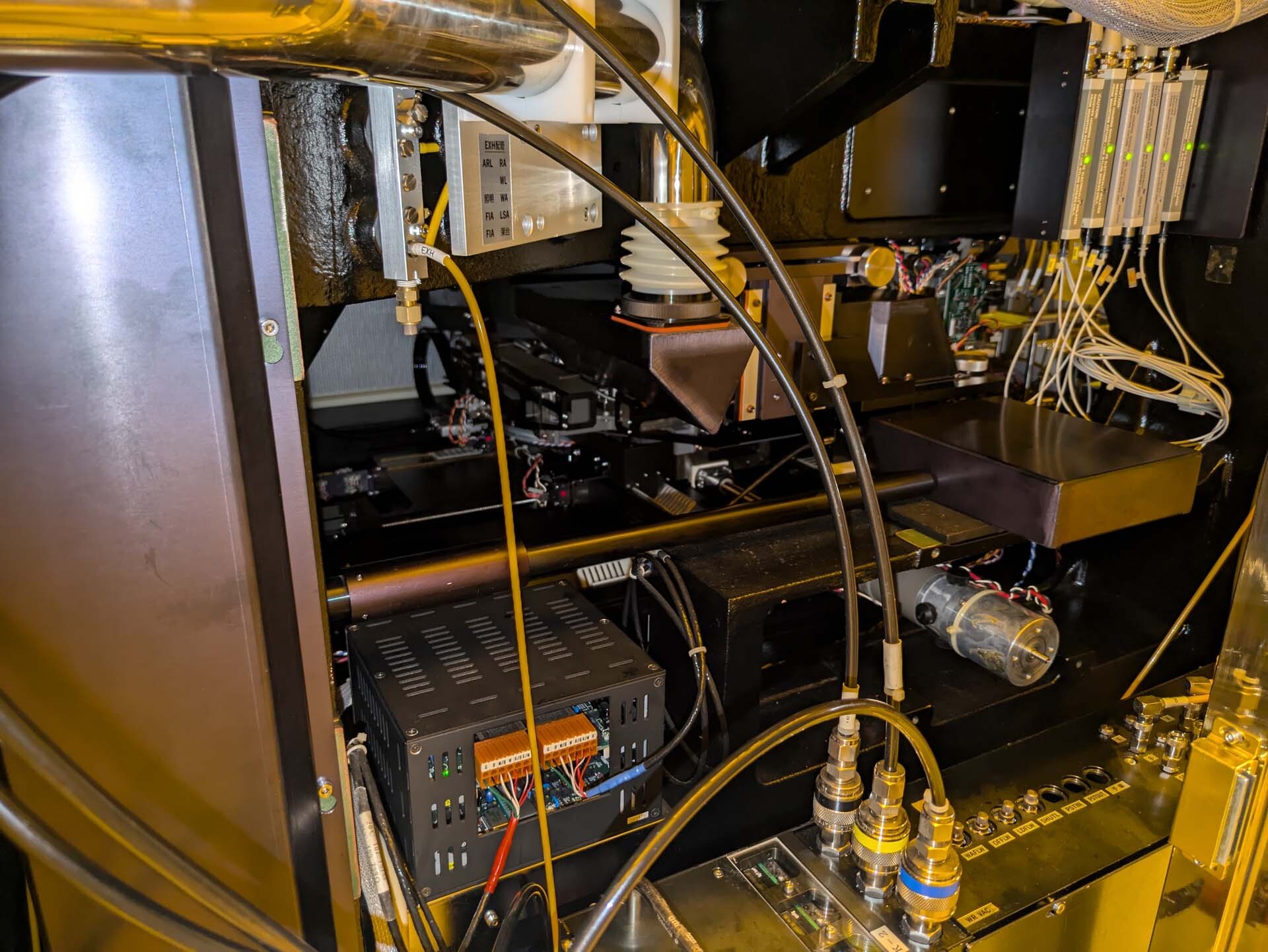
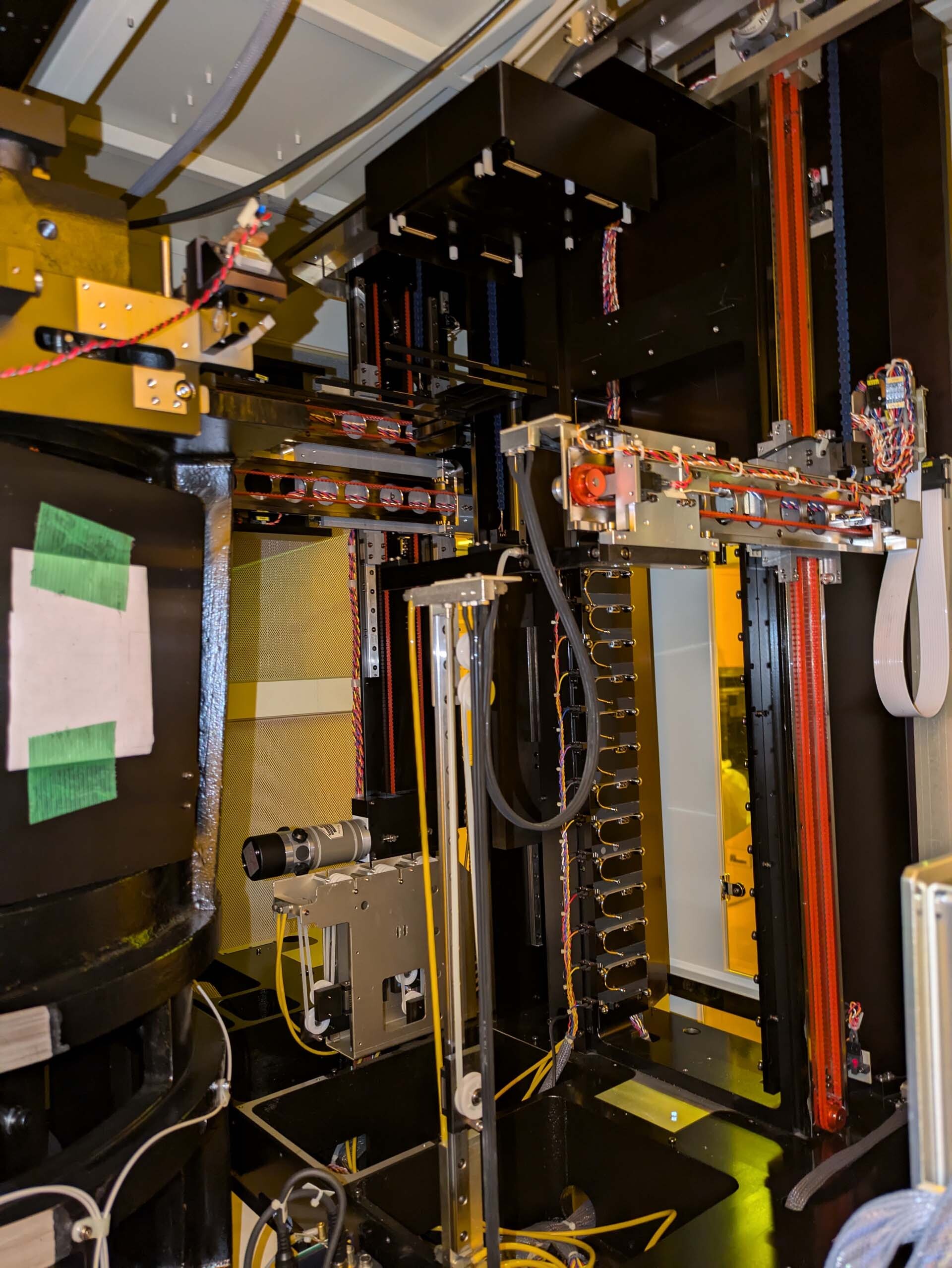
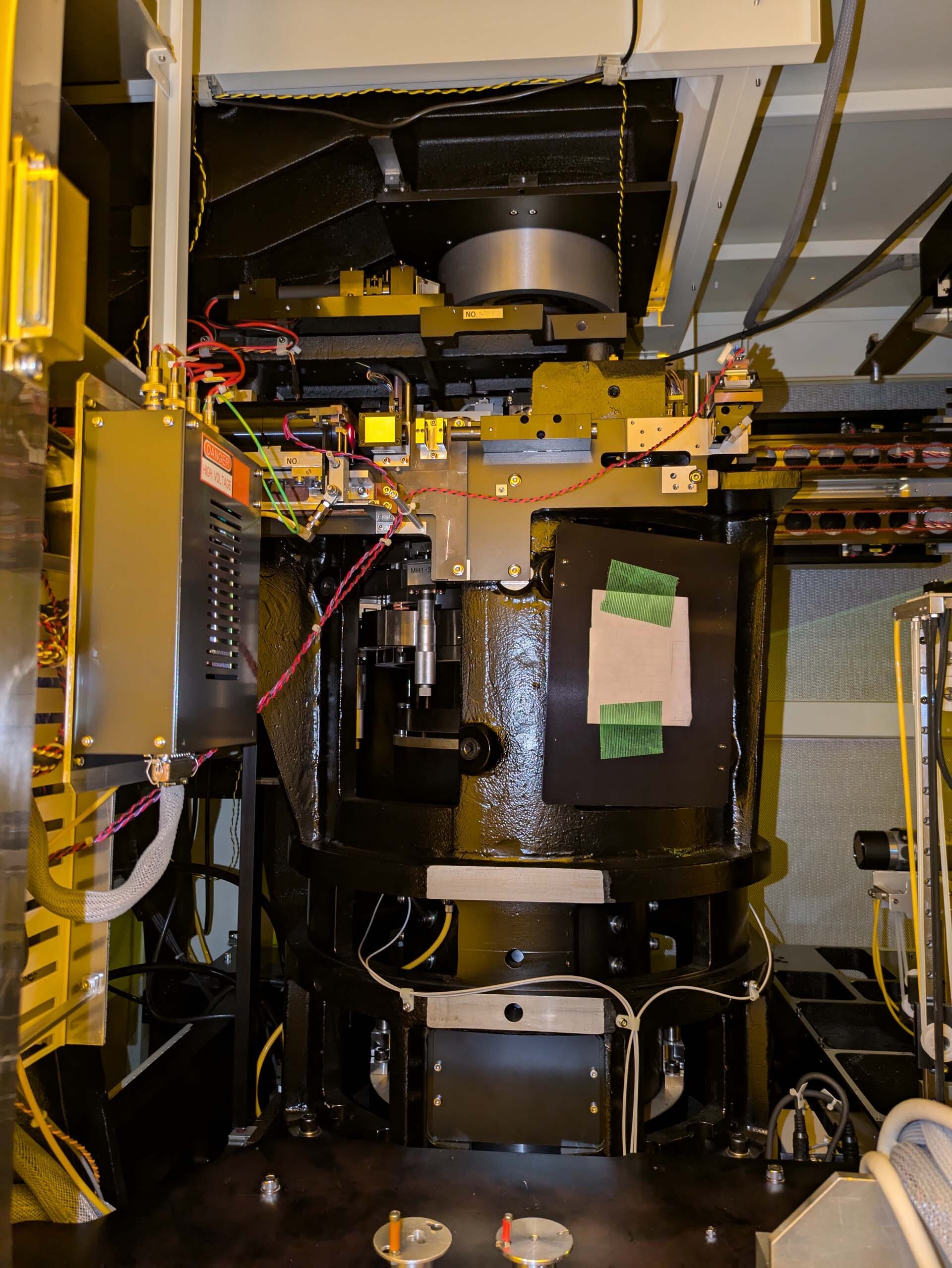
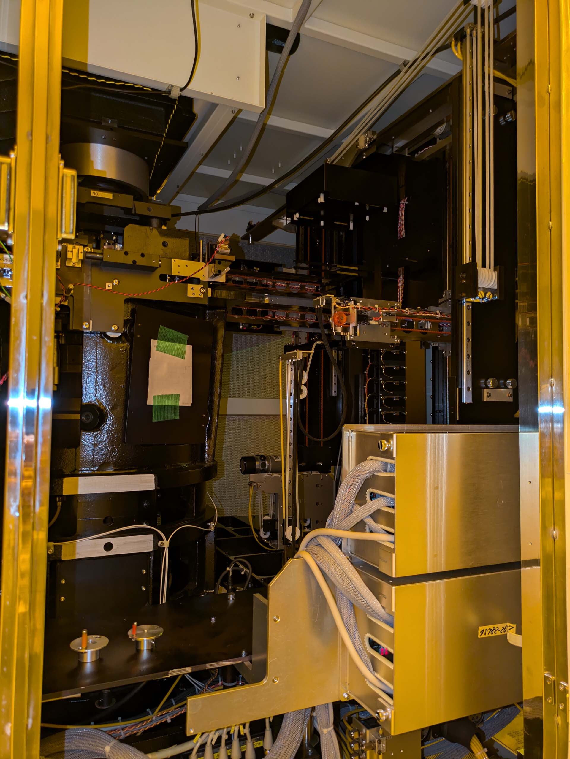
NIKON NSR 4425i is a cutting-edge wafer stepper that is designed to meet the demanding requirements of semiconductor lithography processes. This advanced tool combines precision, speed, and flexibility to enable high-resolution patterning of integrated circuits on silicon wafers at nanometer scales. At the heart of NIKON NSR-4425I lies a sophisticated optical equipment that utilizes a deep ultraviolet (DUV) light source, typically operating at a wavelength of 193 nm. This short wavelength light enables the system to achieve high-resolution patterning, essential for the production of advanced semiconductor devices with densely packed features. NSR 4425 I features a state-of-the-art catadioptric lens unit that plays a crucial role in focusing the DUV light onto the photoresist-coated silicon wafer. The lens machine consists of a combination of mirrors and lenses that work together to minimize optical aberrations and achieve optimal image quality. This ensures that the patterns are accurately transferred from the photomask onto the wafer with exceptional fidelity and resolution. One of the key advantages of NSR 4425i is its advanced alignment and overlay capabilities. The tool is equipped with a sophisticated alignment asset that precisely aligns the patterns on the photomask with the patterns on the wafer, ensuring that the features are placed accurately with respect to each other. This is essential for achieving tight overlay tolerances, which are critical for the performance and functionality of semiconductor devices. In addition to alignment capabilities, NIKON NSR 4425 I offers advanced stage control features that enable precise movement and positioning of the wafer during the exposure process. This high level of control allows for consistent and uniform exposure of the entire wafer, resulting in consistent patterning across the entire surface. NSR-4425I is also equipped with advanced automation capabilities that streamline the lithography process and reduce the risk of human error. The model can be programmed to perform complex exposure sequences automatically, minimizing operator intervention and increasing overall throughput. This automation capability is particularly beneficial for high-volume manufacturing environments where speed and efficiency are critical. Furthermore, NIKON NSR 4425i incorporates advanced monitoring and control systems that continuously monitor key parameters such as exposure dose, focus, and alignment, to ensure optimal process performance and yield. The equipment is designed to provide real-time feedback and adjustments, enabling operators to quickly identify and correct any issues that may arise during the lithography process. Overall, NIKON NSR-4425I represents a state-of-the-art solution for high-resolution semiconductor lithography applications. With its advanced optical system, precision alignment and overlay capabilities, and automation features, the unit enables semiconductor manufacturers to achieve the high levels of patterning accuracy and consistency required for the production of cutting-edge integrated circuits.
There are no reviews yet