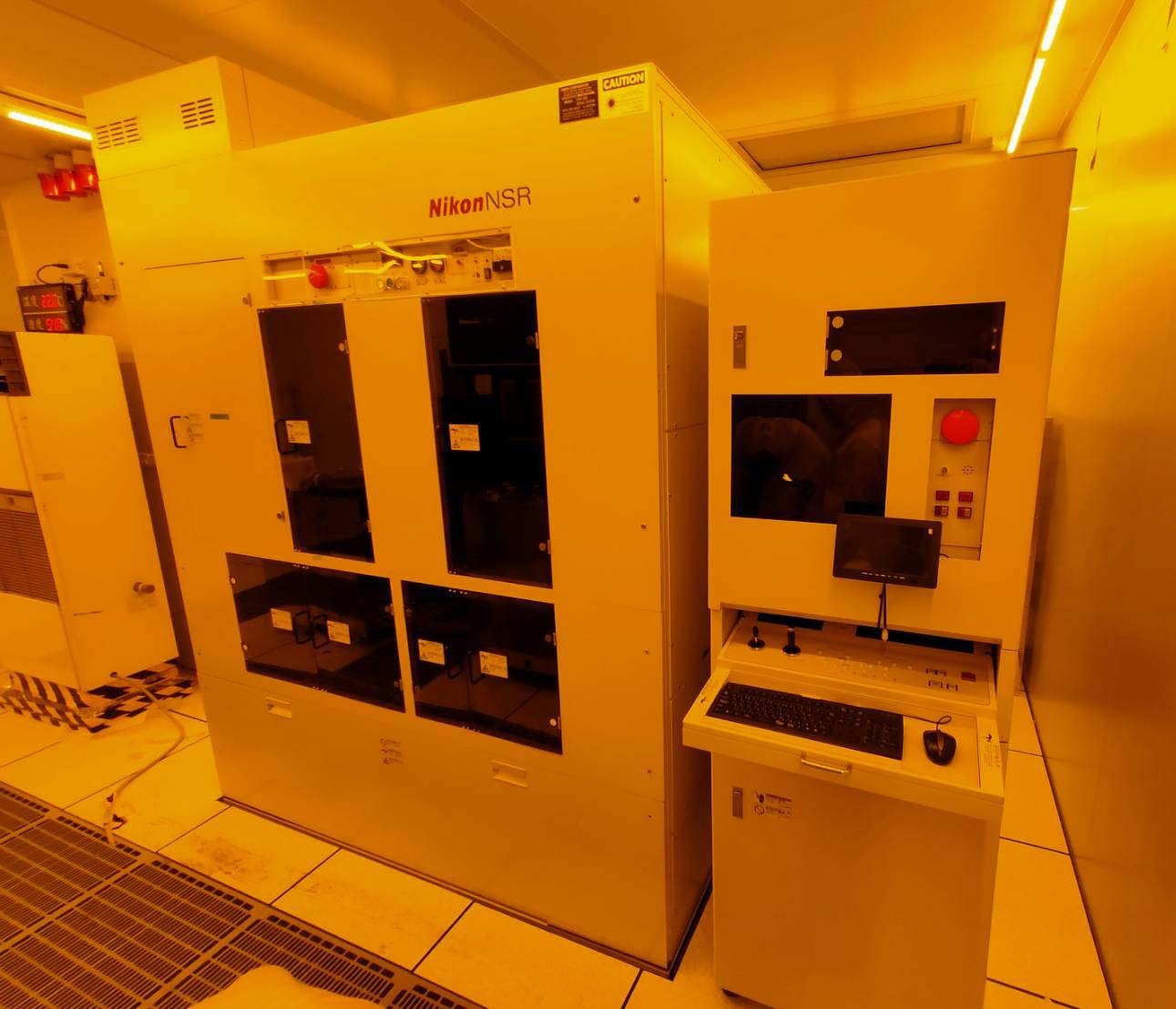
Used NIKON NSR i9 #293586905 for sale
It looks like this item has already been sold. Check similar products below or contact us and our experienced team will find it for you.
Tap to zoom


Sold
ID: 293586905
Stepper
Resolution: 0.5 µm
DOF: 0.7 µm
Expose area: 20 mm
Lens distortion: ±0.10 µm
Exposure power: 500 mW/cm²
Illumination uniformity: <2.0 %
Integrated exp controller: ±2 %
Wafer holder flatness: 2.5 µm
Chip levelling: ±1.5 sec
Auto focus stability range: 0.40 µm (3) times
Stepping accuracy: 0.07 µm
Wafer holder, 8"
Reticle, 6"
Reticle blind: 0.4 - 0.8 mm
Reticle rotation:
Absolute value: ±0.02 µm
Target repeatability value: 0.02 µm.
NIKON NSR i9 is a state-of-the-art wafer stepper capable of accurately and repeatably patterning the surface of large-diameter semiconductor substrates with minimal defectivity. It deftly balances throughput, resolution and cost in a compact, yet highly capable package. NSR i9 employs a 4-lens projection optic to a laser interferometer and navigational equipment, enabling defects as small as 32 nanometers on substrates up to eight inches in diameter. This is twofold an improvement over the system's predecessor. The interferometer allows for sub-nanometer level accuracy in wafer positioning, and the navigational unit enables wafer to wafer alignment accuracy typically limited such operations. NIKON NSR i9 frameset also includes a demagnification lenses, which simultaneously improve the microscope's resolution, and a zoom lens, which magnifies the fields of vision, while maintaining fine focus on a moving target, independently from the substrate position. Other features of NSR i9 include an enhanced laser machine, capable of emitting light of a full spectrum at all process wavelengths, an ultra-low, static and dynamic standoff gap of 1.2 um to 0.1 um respectively, meanwhile ease of use for process changes and optimized for both disk and flat substrates. NIKON NSR i9 also offers cutting-edge features, such as a fully integrated chamber to accommodate both dry and immersion chamber recipes, integrated encapsulation of the optical components in a lightweight design, a digital microscope with a multi-level field of view to identify potential defect, automated tools and settings to minimize substrate handling time and improve mapping quality, while simultaneously preserving safety of the delicate and valuable substrates, allowing NSR i9 to pattern wafers up to 8 inches in diameter with sub-nm accuracy.
There are no reviews yet