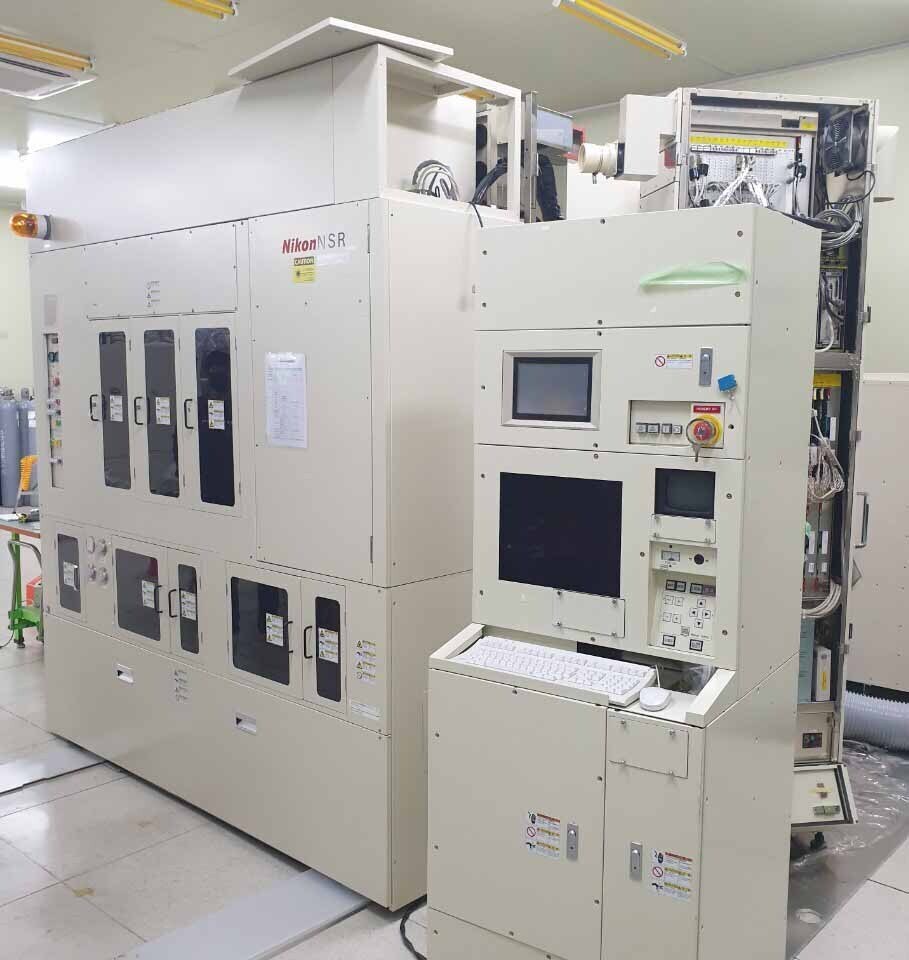
Used NIKON NSR S203B #9357170 for sale
It looks like this item has already been sold. Check similar products below or contact us and our experienced team will find it for you.
Tap to zoom


Sold
ID: 9357170
Wafer Size: 8"
DUV Scanner, 8"
Reticle size, 6"
Wafer loader: Type 3
KOMATSU G10K Laser
Standard BMU
Left in-line
PPD
Bar code reader
Wafer holder flatness: 1.060 um
Field inclination: 0.184 um
Exposure power: 325 mW / cm²
Integrated exposure dose control: 0.45%
Array orthogonality: 0.034 sec
Reticle rotation: 0.004 um
Overlay (LSA):
X: 0.024
Y: 0.042
Overlay (FIA):
X: 0.029
Y: 0.030
Lens distortion:
X: -0.013 ~ 0.019
Y: -0.013 ~ 0.014
Reticle blind setting accuracy:
YF: 0.60, YB: 0.55
XM: 0.60, XP: 0.60
Stepping accuracy:
X: 0.021 um
Y: 0.022 um.
NIKON NSR S203B is a leading-edge wafer stepper designed for advanced lithography processes. It is an immersion-type tool used in semiconductor device manufacturing. The equipment features an optimized optics system, enabling a resolution of 0.13µm, a step size of 0.07µm and a depth of focus of 1.7µm. The unit is a highly integrated, advanced mask aligner capable of producing sub-micron lithography resolution. The machine is equipped with a high-speed 6kW laser auto-focus machine and six-axis auto-leveling control for improved imaging uniformity and accuracy. This helps to ensure that the wafer is accurately placed on the exposure stage and that the optimal focus of exposure is achieved. It also offers an advanced cooling tool with a liquid cooling jacket to prevent the refraction index from changing after the exposure has taken place. The accuracy achieved by this asset is essential to ensure the highest quality of lithography that is possible. NIKON NSR-S203B is designed to offer users a full range of features, including a fully automated exposure operation, a high-precision exposure model and an exposure accuracy level exceeding one percent. The exposure equipment incorporates a resist layer compensation system with a high throughput and low exposure time, to optimize the speed and accuracy of the exposure. The control unit ensures perfect synchronization between the wafer and the exposure unit, and provides the capability to tune exposure parameters. The machine also features a highly efficient temperature-controlled environment chamber to protect the components from exposure to thermal fluctuations. This greatly increases the thermal stability of the device and also reduces potential image errors. Moreover, the tool provides an active vibration control asset, which reduces exposure time to ensure the highest quality imaging. NSR S203B also provides excellent imaging results through the use of advanced algorithms developed for small feature size, high resolution masks and complex exposures. The exposure process is further enhanced with the use of a high resolution camera and advanced image processing algorithms. The camera can detect any dirt or blemishes on the wafer and automatically adjust for them. The model also includes a sophisticated user interface for programming the equipment, enabling users to quickly set up the exposure parameters and parameters. Overall, NSR-S203B wafer stepper provides users with an advanced lithography platform capable of providing high-precision, high-speed, high-throughput and high-accuracy exposure processes. It is designed to be an all-in-one solution for device manufacturers, providing top-notch imaging performance and accuracy.
There are no reviews yet