Used ABONI HydroTracer #293798279 for sale
URL successfully copied!
Tap to zoom
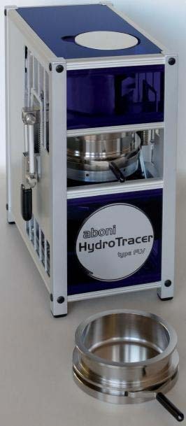

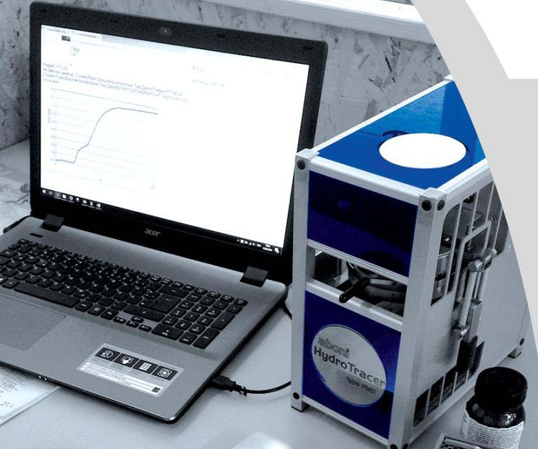
ABONI HydroTracer is a sophisticated wafer testing and metrology equipment designed to provide precise measurements and analysis for semiconductor manufacturing processes. This cutting-edge system incorporates advanced technologies to enable efficient wafer testing and inspection at various stages of the semiconductor fabrication process, ultimately ensuring high quality and reliable semiconductor products. HydroTracer unit utilizes a range of innovative features to achieve its high-performance capabilities. One key aspect of the machine is its hydrostatic measurement technology, which allows for accurate and repeatable measurements of a wafer's thickness, flatness, and other critical parameters. This technology relies on the principle of fluid displacement to provide highly precise measurements, making it an ideal solution for demanding semiconductor manufacturing applications. In addition to hydrostatic measurement, ABONI HydroTracer tool is equipped with state-of-the-art optical inspection capabilities. This includes advanced imaging systems and sensors that can detect defects, particles, and other anomalies on the wafer surface with exceptional sensitivity and resolution. By combining hydrostatic measurements with optical inspection, the asset offers comprehensive metrology capabilities that can help identify and address any issues that may impact the quality and performance of semiconductor devices. Another key feature of HydroTracer model is its automation and control capabilities. The equipment is equipped with advanced software algorithms that enable rapid data processing and analysis, allowing for real-time monitoring of wafer parameters and quick decision-making during the manufacturing process. This automation not only streamlines the testing and metrology process but also enhances overall efficiency and productivity in semiconductor fabrication facilities. Moreover, ABONI HydroTracer system is designed with versatility in mind, making it compatible with a wide range of wafer sizes, materials, and specifications. This flexibility allows semiconductor manufacturers to use the unit across different production lines and processes, adapting to their specific needs and requirements. Whether testing silicon wafers for integrated circuits or compound semiconductor wafers for optoelectronic devices, HydroTracer machine offers a comprehensive solution for precise measurement and quality control. Furthermore, ABONI HydroTracer tool is engineered with reliability and durability in mind, featuring robust construction and components that can withstand the rigors of semiconductor manufacturing environments. This ensures consistent performance and longevity, minimizing downtime and maintenance costs for semiconductor manufacturers. Additionally, the asset is designed with user-friendly interfaces and intuitive controls, making it easy for operators to set up tests, interpret results, and optimize processes for maximum efficiency. In conclusion, HydroTracer model represents a cutting-edge solution for wafer testing and metrology in semiconductor manufacturing. With its advanced technologies, comprehensive metrology capabilities, automation features, and versatility, the equipment offers semiconductor manufacturers a powerful tool to ensure the highest quality and reliability of their semiconductor products. By leveraging the capabilities of ABONI HydroTracer system, manufacturers can optimize their production processes, enhance product quality, and stay competitive in the fast-paced semiconductor industry.
There are no reviews yet