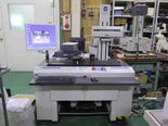
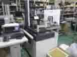
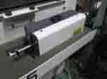
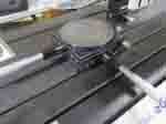
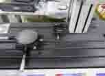
Used ACCRETECH / TSK Surfcom 2000DX #293606726 for sale
URL successfully copied!
Tap to zoom
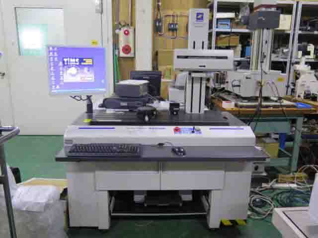

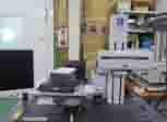

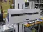





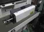

















ID: 293606726
Vintage: 2007
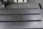
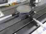
Surface roughness measuring system
TIMS
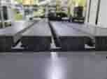
Stone surface plate:1000 x 450 mm
Operating system: Windows XP
Measurement range:
X-Axis: 100 mm
2007 vintage.
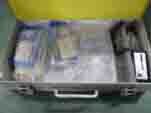
ACCRETECH / TSK Surfcom 2000DX is a wafer testing and metrology equipment that is designed to provide precise measurements of die-to- adjacent surfaces, as well as other substrate characteristics. The system consists of two components: the main unit, and an automated rotary table. The main unit houses a CCD camera and linear stage, which can move across the wafer to measure its characteristics. The rotary table can be used to adjust the angle or tilt of the wafer, enabling the surface topology to be measured in three dimensions. TSK Surfcom 2000DX uses a high-resolution CCD camera, which can capture up to two million pixels. By combining this precision optics with integrated software algorithms, the unit is able to detect and measure features with an accuracy of up to 30nm. This enables it to measure characteristics such as linewidths, trenches, step height, transverse surface roughness, and inter-layer dielectric fills. The unit also features an image-processing machine that can process multiple images in real-time. This tool combines digital image-processing techniques with advanced pattern recognition algorithms to extract critical measurements from the wafer images. The software also includes a powerful visualization asset that displays the captured images and measurements in 2D and 3D formats. The model is also capable of performing Die-to-Film (DTF) comparison and analysis. This process enables accurate comparison of the substrate surface features to topographical patterns saved in a "film library". Finally, the equipment supports a wide range of metrology functions, such as stress testing, analysis of integrated circuits, measurement of coating thickness, and non-contact wafer mapping. Overall, ACCRETECH Surfcom 2000DX is a powerful wafer testing and metrology system capable of providing precise measurements of die-to-adjacent surfaces and other substrate features. Its combination of optics and software algorithms enable it to capture and analyze images with an accuracy of up to 30nm, while its pattern recognition algorithms and visualization tools allow users to quickly analyze the data. Finally, the unit is capable of performing DTF comparison and analysis to determine the precise topography of the wafer.
There are no reviews yet
