Used AMAT / APPLIED MATERIALS NANOSEM 3D #9121584 for sale
URL successfully copied!
Tap to zoom


ID: 9121584
Wafer Size: 12"
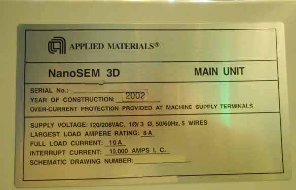
Vintage: 2002
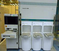
Critical Dimension Scanning Electron Microscope (CD SEM), 12"
Install type: Stand alone
(3) Cassette interface: FOUP, 12"
Roll-around ergo station with touch screen
Status lamp
Options:
Slope reconstruction
CH analysis
Profile grade
Discrete inspection
Defect review
ARAMS (ES8)
CE Marked
Power requirements: 120/208 V, 8 A, Single phase / 3 Phase, 5-Wire, 50/60 Hz
2002 vintage.
AMAT / APPLIED MATERIALS NANOSEM 3D is an advanced wafer testing and metrology equipment incorporating key technology for nanoscale monitoring and process control. AMAT NANOSEM 3D enables precise measurement of patterns down to <10 nm and accurate 3D imaging at the nanoscale over large areas. It is used to evaluate a variety of materials and processes, including processing, metrology, and defect analysis in a wide range of semiconductor, optoelectronics, and nano materials applications. APPLIED MATERIALS NANOSEM 3D system combines patented lithography/line degradation analysis (LDA) with onboard electron microscopy (EM) tomography and automated material analysis tools. The unit provides complete 3D field-of-view (FOV) images that reveal accurate details of both 2D and 3D structures, as well as line edge roughness (LER) measurements. The LDA technology provides advanced, automated capabilities for detecting edge roughness and can detect, quantify, and characterize even minute features down to a few nanometers. NANOSEM 3D systems feature a fully automated image capture capability, high throughput performance, and real-time visualization of data. The machine includes an easy-to-use user interface with wizards and guides that enable efficient, convenient operation. It also features a wide range of advanced features, including both remote and local operation, high-resolution images, 4-D imaging, and specialized analysis tools. AMAT / APPLIED MATERIALS NANOSEM 3D tool is designed to optimize process flow and reduce analysis time while providing high-quality, detailed data. The integrated platform enables the analysis of large areas of patterns over an extended scanning depth, allowing full view of 3D structures in an integrated manner. In addition, the asset enables precise analysis of data collected during the testing operation and provides precise image resolution at each stage. AMAT NANOSEM 3D systems are suitable for a variety of applications, such as metrology and metrology-assisted process control, defect detection and analysis, line edge roughness measurements, and line width measurements. This model is ideal for use in semiconductor, optoelectronics, and nano materials production processes. Additionally, the equipment is well suited for customized solutions for specific applications. APPLIED MATERIALS NANOSEM 3D provides state-of-the-art solutions for accurate and reliable test information.
There are no reviews yet

